Supercharge Your Innovation With Domain-Expert AI Agents!

Automatic quality classifying device and method for solar polycrystalline silicon chips

A polycrystalline silicon wafer, automatic sorting technology, applied in sorting and other directions, can solve the problems of low intelligence, low detection quality, low work efficiency, etc., to improve the degree of mechanization, improve work efficiency, and reduce manual screening.

Pending Publication Date: 2018-09-28
JIAXING NENGFA ELECTRONICS TECH CO LTD
View PDF7 Cites 0 Cited by
  • Summary
  • Abstract
  • Description
  • Claims
  • Application Information

AI Technical Summary

Problems solved by technology

[0005] An automatic classification device and classification method for the quality of solar polycrystalline silicon wafers of the present invention are used to solve the problems of low intelligence, low work efficiency, low detection quality, and detection and classification costs raised in the above-mentioned background technology

Method used


Image

  • Automatic quality classifying device and method for solar polycrystalline silicon chips
  • Automatic quality classifying device and method for solar polycrystalline silicon chips
  • Automatic quality classifying device and method for solar polycrystalline silicon chips

Examples


Embodiment Construction

[0021] The following will clearly and completely describe the technical solutions in the embodiments of the present invention with reference to the accompanying drawings in the embodiments of the present invention. Obviously, the described embodiments are only a part of the embodiments of the present invention, rather than all the embodiments. The embodiments in the invention, and all other embodiments obtained by those of ordinary skill in the art without creative work, fall within the protection scope of the invention.

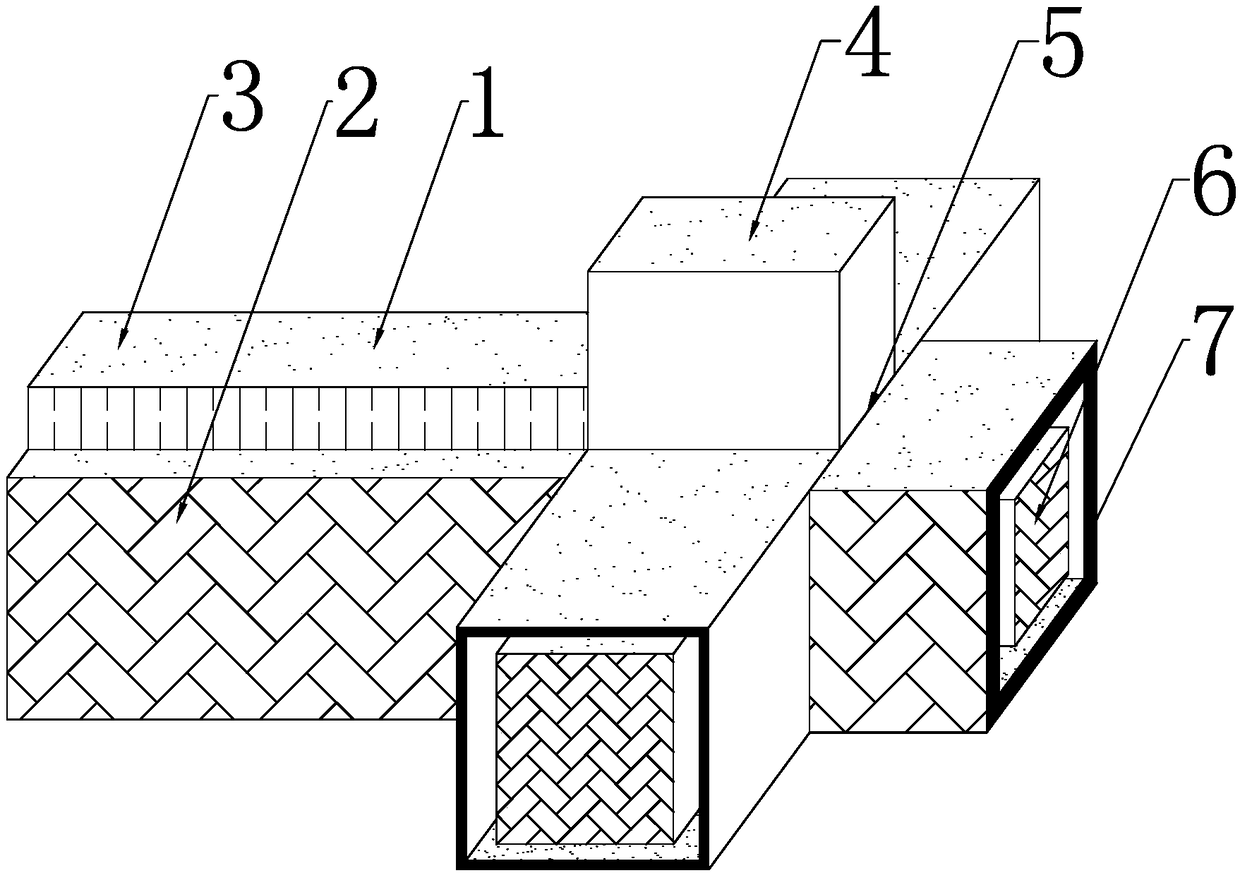
[0022] See Figure 1-3 , The present invention provides a technical solution: an automatic quality classification device for solar polycrystalline silicon wafers, including a device main body 1, a detection device 2 and a summarizing device 5. The left end of the device main body 1 is provided with a detection device 2, the detection device 2 and the device main body 1. Electrically connected, the top of the detection device 2 is provided with an organic top co...


PUM


Abstract

The invention provides an automatic quality classifying device and method for solar polycrystalline silicon chips, and belongs to the technical field of solar energy. The problem that existing solar polycrystalline silicon chips are not prone to being classified is solved. The automatic quality classifying device for the solar polycrystalline silicon chips comprises a device main body, a detectingdevice and an arranging device; the detecting device is arranged at the left end of the device main body and electrically connected with the device main body; a machine top cover is arranged at the top end of the detecting device and fixedly connected with the detecting device; the arranging device is arranged at the right end of the device main body and electrically connected with the device main body; and a storage cabinet is arranged at the right end of the arranging device and connected with the arranging device in a penetrating mode. The automatic quality classifying device for the solarpolycrystalline silicon chips integrates detecting and classifying, thus the two working procedures of detecting and classifying are completed simultaneously, and the working efficiency of the automatic quality classifying device is greatly improved.

Description

Technical field [0001] The invention relates to the technical field of quality detection and classification, in particular to an automatic quality classification device and a classification method for solar polycrystalline silicon wafers. Background technique [0002] Polycrystalline silicon wafer is a form of elemental silicon. When molten elemental silicon solidifies under supercooling conditions, silicon atoms are arranged into many crystal nuclei in the form of a diamond lattice. If these crystal nuclei grow into crystal grains with different crystal plane orientations, these crystal grains combine to crystallize into polysilicon , Polycrystalline silicon wafers are mostly used in electronics and solar power generation. They are used as raw materials in the solar energy industry chain. They are used to cast ingots or pull monocrystalline silicon rods, cut into silicon wafers, and produce solar panels. [0003] Nowadays, the quality classification of polycrystalline silicon waf...

Claims


Application Information

Patent Timeline
IPC IPC(8): B07C5/34B07C5/36
CPCB07C5/34B07C5/361B07C5/362
Inventor 高峰朱晴峰李有钱其峰
Owner JIAXING NENGFA ELECTRONICS TECH CO LTD
Features
  • R&D
  • Intellectual Property
  • Life Sciences
  • Materials
  • Tech Scout
  • Unparalleled Data Quality
  • Higher Quality Content
  • 60% Fewer Hallucinations
Learn More