Fingerprint module and electronic device

A fingerprint module and fingerprint identification technology, which is applied in the direction of acquiring/organizing fingerprints/palmprints, character and pattern recognition, instruments, etc., can solve problems such as the thickness of fingerprint modules, and achieve thickness saving, thickness reduction, and thinning The effect of the design

Pending Publication Date: 2018-09-28
昆山丘钛生物识别科技有限公司
View PDF0 Cites 4 Cited by
  • Summary
  • Abstract
  • Description
  • Claims
  • Application Information

AI Technical Summary

Problems solved by technology

[0004] In view of this, the purpose of the embodiments of the present invention is to provide a fingerprint module and electronic equipment to improve the existing thick fingerprint module problem

Method used


Image

  • Fingerprint module and electronic device
  • Fingerprint module and electronic device
  • Fingerprint module and electronic device

Examples


no. 1 example

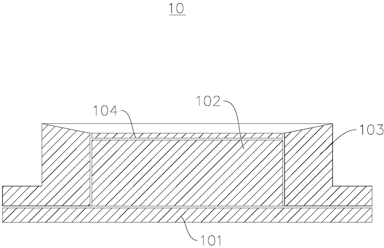
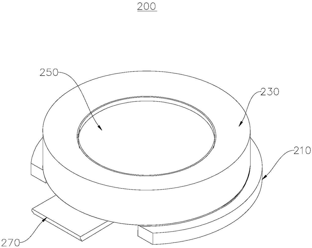
[0040] This embodiment provides a fingerprint module 200 to solve the problem that the existing fingerprint module 200 has a lot of stacked thicknesses and cannot be reduced in thickness. see figure 2 and image 3 , figure 2 A schematic diagram of the stacked structure of the fingerprint module 200 provided in this embodiment is shown.

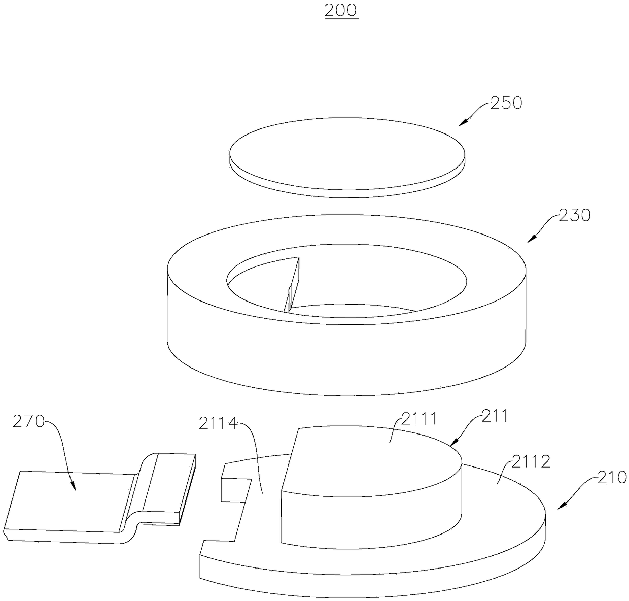
[0041] image 3 An exploded view of the fingerprint module 200 provided in this embodiment is shown. The fingerprint module 200 includes a module circuit substrate 270 , a fingerprint identification chip 210 , a protection ring 230 and a cover 250 . The module circuit substrate 270 is electrically connected to the fingerprint recognition chip 210 , the protection ring 230 is bonded to the fingerprint recognition chip 210 , and the cover plate 250 is bonded to the protection ring 230 and the fingerprint recognition chip 210 .

[0042] see Figure 4 and Figure 5 , the fingerprint identification chip 210 includes a first plane 2111 and ...

no. 2 example

[0058] This embodiment provides an electronic device 30, please refer to Figure 10 , the electronic device 30 includes a device body 300 and the fingerprint module 200 provided in the first embodiment, and the fingerprint module 200 is connected to the device body 300 . The electronic device 30 includes, but is not limited to, a mobile phone, a tablet computer, a notebook computer, and the like. For example, the fingerprint module 200 can be disposed on any flat or curved surface of the electronic device 30 . The fingerprint module 200 includes a module circuit substrate 270 , and the module circuit substrate 270 is used to realize the electrical connection between the fingerprint identification chip 210 and the device body 300 , so as to transmit information such as the identified fingerprint to the device body 300 .

[0059] In summary, the present invention provides a fingerprint module and electronic equipment. The fingerprint module includes a fingerprint identification...


PUM


Abstract

The present invention provides a fingerprint module and an electronic device, and relates to the technical field of fingerprint modules. The fingerprint module comprises a fingerprint identification chip and a module circuit substrate. The fingerprint identification chip comprises a first plane and a second plane which form a stepped structure, wherein the first plane protrudes from the second plane; the fingerprint identification chip further comprises a connecting surface and a mounting port, wherein the connecting surface is formed on the second plane, and the mounting port is formed on thearea of the second plane near the connecting surface; and the module circuit substrate comprises a connecting portion, wherein the connecting portion passes through the mounting port and is electrically connected with the connecting surface. Compared with the conventional fingerprint module structures, the fingerprint module provided by the present invention is arranged on the stepped structure of the fingerprint identification chip through the area where the fingerprint identification chip and the module circuit substrate are connected, so that the thickness of the module circuit substrate and the thickness of the conductive material are saved, the thickness of the fingerprint module is reduced, and the thin and light design of the electronic device can be implemented in a facilitated manner.

Description

technical field [0001] The invention relates to the technical field of fingerprint modules, in particular to a fingerprint module and electronic equipment. Background technique [0002] With the rapid development of the mobile Internet era, the information interaction between mobile terminal users is also increasing exponentially. At the same time, various telecommunication frauds and identity information theft incidents occur frequently, and the identification technology security issues of user ID information It has become a hot topic of much attention. In the mobile Internet interaction, biometric technology has become an emerging interactive technology under the leadership of the times and is gradually recognized by the public. Fingerprint recognition technology has become a standard configuration in mobile phones. . [0003] The traditional fingerprint module structure includes a cover plate, a metal ring, a fingerprint chip, and a module circuit substrate. The fingerpr...

Claims


Application Information

Patent Timeline
Patent Type & Authority Applications(China)
IPC IPC(8): G06K9/00
CPCG06V40/12G06V10/94
Inventor 邹兵陈亮
Owner 昆山丘钛生物识别科技有限公司
Why Eureka
Try Eureka