A chip-type high-voltage silicon stack and its production process

A high-voltage silicon stack and SMD technology, applied in the field of diodes, can solve problems such as easy bending and damage to electrode leads, and achieve the effect of preventing bending and improving service life

Active Publication Date: 2020-07-28
RUGAO DACHANG ELECTRONICS
View PDF15 Cites 0 Cited by
  • Summary
  • Abstract
  • Description
  • Claims
  • Application Information

AI Technical Summary

Problems solved by technology

[0003] However, there is no protective mechanism on the body of the general high-voltage silicon stack. Since the electrode leads are welded on the body of the high-voltage silicon stack, it is easy to be bent during transportation, resulting in damage to the electrode leads. Chip-type high-voltage silicon stack and its production process to solve the protection problem of electrode leads, improve its service life, and help prevent electrode leads from being bent and damaged during transportation

Method used


Image

  • A chip-type high-voltage silicon stack and its production process
  • A chip-type high-voltage silicon stack and its production process
  • A chip-type high-voltage silicon stack and its production process

Examples


Embodiment Construction

[0025] The following will clearly and completely describe the technical solutions in the embodiments of the present invention with reference to the accompanying drawings in the embodiments of the present invention. Obviously, the described embodiments are only some, not all, embodiments of the present invention. Based on the embodiments of the present invention, all other embodiments obtained by persons of ordinary skill in the art without making creative efforts belong to the protection scope of the present invention.

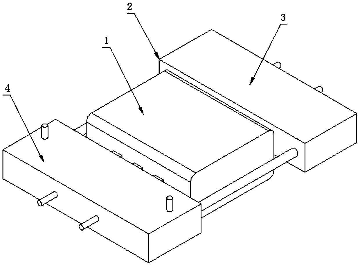
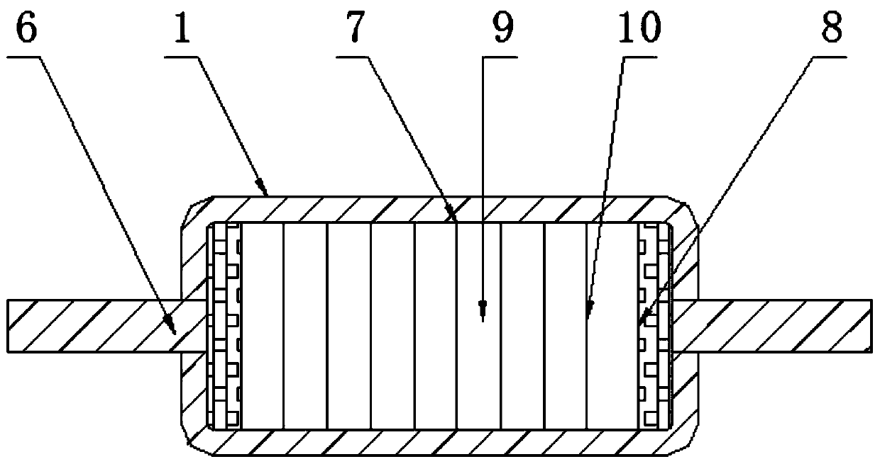
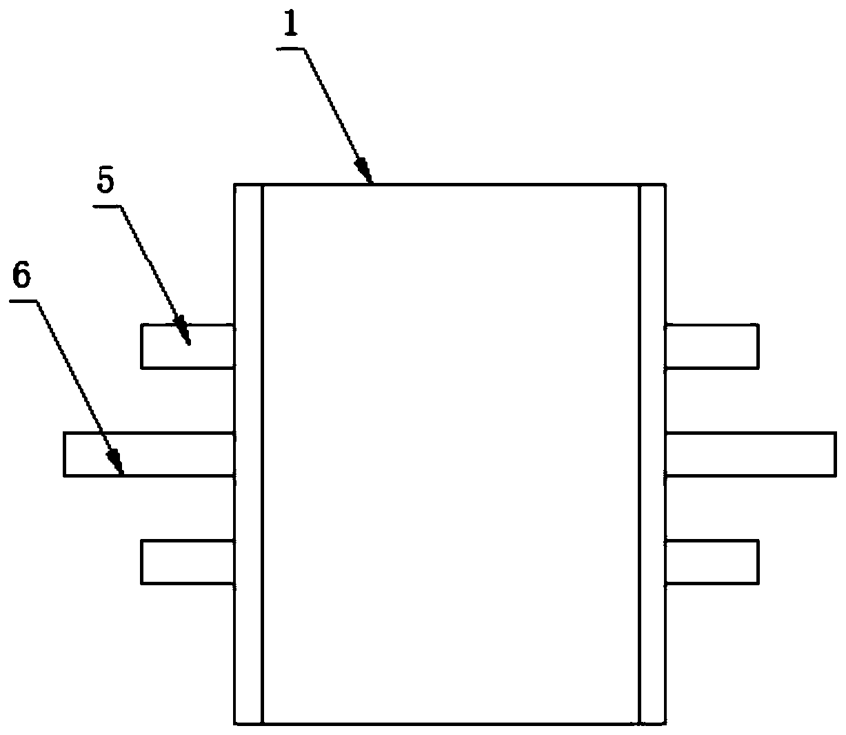
[0026] see Figure 1-7, the present invention provides a chip-type high-voltage silicon stack, including a high-voltage silicon stack body 1 and a protection mechanism 2, and the high-voltage silicon stack body 1 is composed of an insertion rod 5, an electrode lead 6, a protective cover 7, a tungsten electrode 8, and a tube core 9 , two tungsten electrodes 8 are provided, the electrode leads 6 are welded on one side of the tungsten electrode 8, the tube core 9...


PUM


Abstract

The invention discloses a patch type high-voltage silicon stack and a producing process thereof. The patch type high-voltage silicon stack comprises a high-voltage silicon stack body and a protectingmechanism. Two tungsten electrodes are arranged, electrode leads are welded to one sides of the tungsten electrodes, a tube core is formed by connecting a plurality of chips in series, and the tungsten electrodes are welded at the two corresponding ends of the tube core. The tube core is sleeved with a protecting cover, the tungsten electrodes are located at the centers of the two corresponding ends of two corresponding sides of the protecting cover, and inserting rods are bonded at the positions, located at the two corresponding ends of the tungsten electrodes, of the two corresponding sidesof the protecting cover. The protecting mechanism is composed of a right fixing plate, a left fixing plate, cubic fixing blocks, buffering rods, pull rods, connecting rods, cubic fixing grooves, sliding grooves, first through holes, first reset springs, clamping blocks, inserting grooves, lead grooves, a buffering plate, second through holes, second reset springs and a sponge mat. The high-voltagesilicon stack can protect the electrode leads and prevent the electrode leads from being damaged during transportation.

Description

technical field [0001] The invention relates to the technical field of diodes, in particular to a chip-type high-voltage silicon stack and a production process thereof. Background technique [0002] The high-voltage silicon stack is also called a silicon column. It is a silicon high-frequency high-voltage rectifier diode with an operating voltage of several thousand volts to tens of thousands of volts. It is often used for high-frequency and high-voltage rectification in black and white TV sets or other electronic instruments. The reason why it can withstand such a high voltage is that its interior is composed of several silicon high-frequency diode cores connected in series. , The outside is packaged with high-frequency ceramics. [0003] However, there is no protective mechanism on the body of the general high-voltage silicon stack. Since the electrode leads are welded on the body of the high-voltage silicon stack, it is easy to be bent during transportation, resulting in...

Claims


Application Information

Patent Timeline
Patent Type & Authority Patents(China)
IPC IPC(8): H01L23/00H01L25/07H01L21/52
CPCH01L21/52H01L23/562H01L25/074
Inventor 王志敏黄丽凤
Owner RUGAO DACHANG ELECTRONICS
Why Eureka
Try Eureka