Surface test method based on atomic scattering

A surface testing and atomic technology, applied in measurement devices, instruments, scanning probe microscopy, etc., can solve problems such as affecting beam current characteristics, cumbersome steps, affecting experimental progress, etc., to change the beam spot size and increase the range. , Simple operation and time-saving effect

Pending Publication Date: 2018-10-16
JINHUA VOCATIONAL TECH COLLEGE
View PDF5 Cites 0 Cited by
  • Summary
  • Abstract
  • Description
  • Claims
  • Application Information

AI Technical Summary

Problems solved by technology

Defect 1 of the existing technology: the distance between the splitter and the injection head will affect the beam characteristics, but at present, there is no atomic beam microscopic device that can realize the precise adjustment of the distance between the splitter and the injection head
Defect 2 of the existing technology: To study the different characteristics of different samples needs to make the atomic beam microscope work at different resolutions. However, if the resolution of the atomic beam microscope is to be changed in the experiment, it is necessary to destroy the vacuum environment of the device to replace the components , the steps are cumbersome and affect the progress of the experiment, the surface test method based on atomic scattering can solve the problem

Method used


Image

  • Surface test method based on atomic scattering

Examples


Embodiment Construction

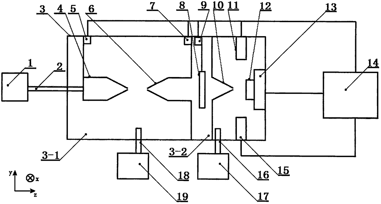
[0023] Such as figure 1It is a schematic diagram of the surface testing device based on atomic scattering in the present invention. The surface testing device based on atomic scattering mainly includes a gas storage tank (1), a gas pipe (2), a cavity I (3-1) and a cavity II (3-2 ) connected to form a vacuum chamber (3), injection head (4), driver I (5), shunt (6), driver II (7), collimating aperture array (8), translation stage (9), main Aperture (10), detector I (11), sample (12), sample stage (13), computer (14), detector II (15), suction port I (16), vacuum pump group I (17), suction Gas port II (18), vacuum pump group II (19), xyz is a three-dimensional coordinate system, and the z-axis is a horizontal direction. The cavity I (3-1) and cavity II (3-2) pass through the flow divider (6) Connection, the cavity II (3-2) is connected to the vacuum pump group I (17) through the suction port I (16), and the cavity I (3-1) is connected to the vacuum pump group II (19) through the...


PUM


Abstract

The invention relates to the technical field of material microscopy. The surface test method based on atomic scattering comprises the steps that a vacuum pump set is started to vacuumize cavity bodies, so that vacuum degree in a cavity body I is greater than 10-1Pa, and vacuum degree in a cavity body II is greater than 10-2 Pa; an air storage tank outputs air to an ejecting head, air atoms enter the cavity I in a free jetting manner, and after the air atoms pass through a diverter, the air atoms in an atomic beam form enter the cavity body II; the atomic beams successively pass through a collimating aperture array and a main aperture to the surface of a sample; a displacement platform is controlled to move to adjust the position of the collimating aperture array, so that the required apertures are located on an atomic beam path; a detector I and a detector II detect partial atoms reflected by the sample surface, the signal intensity is obtained through a computer, positions of the ejecting head and diverter are adjusted, and a sample table translates within a 1*1 micron range; the partial atoms reflected by the sample surface enter the detectors, the obtained data is input in the computer, the computer processes the data, and relevant information of the sample surface is obtained.

Description

technical field [0001] The invention relates to the field of microscopic technology for materials, especially a surface testing method based on atomic scattering, which has a specially designed collimated aperture, and the distance between the spray head and the flow divider can be automatically adjusted according to the intensity of the atomic beam . Background technique [0002] In the field of microscopic technology, general electron microscopes can only image conductive samples, and the energy of the electron beam emitted by the electron microscope is relatively high, which will cause some sensitive sample surfaces to be damaged by radiation. The atomic beam microscope can overcome the above defects and image fragile or insulating samples. It usually uses inert gas atoms as the emitting atoms. The energy of the atomic beam of the inert gas is very low and its chemical properties are very stable. Obtain an image of the surface of the sample. The working principle of the...

Claims


Application Information

Patent Timeline
Patent Type & Authority Applications(China)
IPC IPC(8): G01Q60/24
CPCG01Q60/24
Inventor 张向平赵永建
Owner JINHUA VOCATIONAL TECH COLLEGE
Why Eureka
Try Eureka