
Novel lightning plug and manufacturing method thereof

A plug, a new type of technology, applied in the direction of fixed connection, fixed/insulated contact components, circuits, etc., can solve the problems of PIN position easy to fall off, difficult welding operation, low welding efficiency, etc., to achieve convenient welding operation and high welding accuracy , The effect of improving welding efficiency

Pending Publication Date: 2018-10-19
东莞市杰讯电子科技有限公司
View PDF7 Cites 0 Cited by
  • Summary
  • Abstract
  • Description
  • Claims
  • Application Information

AI Technical Summary

Problems solved by technology

[0005] However, the existing lightning plug, because the gap between the PIN pads on the PCB is small, is difficult to fix when welding the wires, the welding operation is difficult, and the welding efficiency is low; the welded wires are not fixed, if the wires are on the There is swing during transportation, and the soldered PIN is easy to fall off; in addition, during the welding operation, since the electronic components of the PCB board are exposed, it is inevitable that the human hands will touch the electronic components. At this time, the static electricity of the human body may be Break down the MOS tube of the electronic component
[0006] Based on the above reasons, the defective rate of lightning plug processing in the industry can only be controlled at 3% or above. How to overcome the industry's technological bottleneck to further reduce the defective rate of lightning plug processing has become a technical problem that technicians in the field urgently need to solve.

Method used


Image

  • Novel lightning plug and manufacturing method thereof
  • Novel lightning plug and manufacturing method thereof
  • Novel lightning plug and manufacturing method thereof

Examples

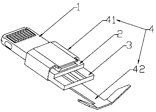
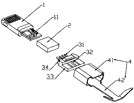
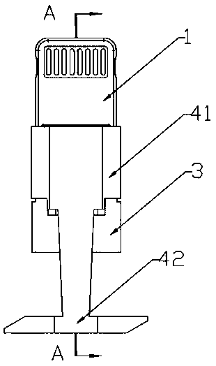

Embodiment Construction

[0026] The following are only preferred embodiments of the present invention, and therefore do not limit the protection scope of the present invention.

[0027] Figure 1-Figure 4 A new type of lightning plug 1 shown includes a lightning plug 1, a protective layer 2, an adapter part 3 and a wire fixing part 4. One end of the lightning plug 1 is provided with a PCB board 11, and the surface of the PCB board 11 is provided with electronic components. The back is provided with a number of PIN pads 12 arranged in sequence,

[0028] The protective layer 2 is made of low-pressure injection molding material, and is injected on the surface of the PCB board 11 through a low-pressure injection molding process to protect the electronic components on the surface of the PCB board 11; the protective layer 2 is injected using a low-pressure injection molding process to avoid damage to the PCB board during the injection molding process The electronic components on the surface of 11, after in...


PUM


Abstract

The invention discloses a novel lightning plug, which comprises a lightning plug. One end of the lightning plug is provided with a PCB (printed circuit board), an electronic element is arranged on thesurface of the PCB, and a plurality of PIN bit bonding pads which are sequentially arranged are arranged on the back surface of the PCB. The novel lightning plug also comprises a protection layer, which is injected on the surface of the PCB through the technology of low-pressure injection molding for protecting the electronic element on the surface of the PCB; a switching component, which is fixedly connected with the PCB, wherein a pin corresponding to the PIN bit bonding pad is arranged at one end of the switching component, the pin is fixed to the corresponding PIN bit bonding pad in a welding mode, and the other end of the switching component is provided with a welding piece which is integrally formed with the pin and is used for being welded with a wire; a wire fixing part, which isconnected with the lightning plug, and fixes the wire welded on the welding piece through a clamping mode. The invention is advantageous in that the processing efficiency is high, the industry bottleneck is broken through, and the defective product rate is only 0.1%.

Description

technical field [0001] The invention relates to the technical field of connectors, in particular to a novel lightning plug and a manufacturing method thereof. Background technique [0002] Lightning plug, also known as lightning plug, is an exclusive connector specification made by Apple; in addition to basic charging and data transmission, it also supports digital signal output functions such as video and audio. [0003] The existing data cable with the Lightning plug includes two parts, the lightning plug and the wire. The lightning plug part is provided by a manufacturer specified by Apple, and its structure is fixed. [0004] One end of the lightning plug is provided with a PCB board, and a PIN pad is provided on the PCB board. During the production process, the core wires in the wires are respectively welded to the PIN pads, and then a layer of outer mold is injected on the surface of the PCB board. , the finished product can be obtained. [0005] However, the existin...

Claims


Application Information

Patent Timeline
Patent Type & Authority Applications(China)
IPC IPC(8): H01R12/57H01R13/40
CPCH01R12/57H01R13/40
Inventor 余安云张美群
Owner 东莞市杰讯电子科技有限公司
Learn More