On-chip integrated transceiver matching network and method suitable for constant envelope non-linear modulation

A matching network, nonlinear technology, applied in the field of on-chip antenna matching circuit

Active Publication Date: 2018-10-19
上海亮牛半导体科技有限公司
View PDF7 Cites 6 Cited by
  • Summary
  • Abstract
  • Description
  • Claims
  • Application Information

AI Technical Summary

Problems solved by technology

At present, there is a lack of an on-chip antenna matching circuit that can effectively filter out high-order harmonic components in a constant-envelope nonlinear modulation communication mode

Method used


Image

  • On-chip integrated transceiver matching network and method suitable for constant envelope non-linear modulation
  • On-chip integrated transceiver matching network and method suitable for constant envelope non-linear modulation
  • On-chip integrated transceiver matching network and method suitable for constant envelope non-linear modulation

Examples


Embodiment Construction

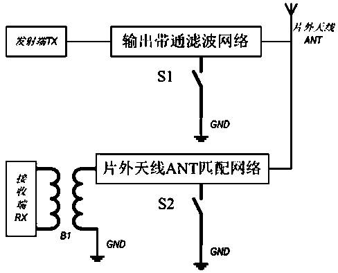
[0049] Such as figure 1 As shown, the present invention provides a novel on-chip matching network whose topology structure includes: an output bandpass filter network, an antenna matching network, an on-chip transformer B1, a switch S1 and a switch S2. The off-chip antenna ANT in the figure is an off-chip component of the integrated circuit, and the others are implemented on-chip.

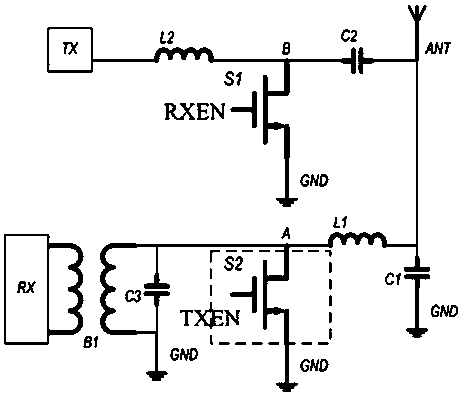
[0050] figure 2 Show the first embodiment of the on-chip matching network of the present invention:

[0051] The output of the transmitter TX in the integrated circuit is connected to one end of the inductor L2 on the chip, and the other end of the inductor L2 is connected to the drain end of the switch S1 of the NMOS transistor and a plate of the capacitor C2 on the chip at node B, and the source end of the switch S1 is connected to GND. Its gate is controlled by receiving the enable signal RXEN. The other plate of the capacitor C2 is connected with one plate of the on-chip capacitor C1, conne...


PUM


Abstract

The invention provides an on-chip integrated transceiver matching network and method suitable for constant envelope non-linear modulation. The method comprises the following steps that: when a chip isin a receiving state, a first toggle switch is switched on, so that no signal connection exists between a transmitting end TX of an on-chip transmitting circuit and a port of an off-chip antenna, a second toggle switch is switched off, and a signal of an antenna port is transmitted to a receiving end RX of an on-chip receiving circuit through an antenna matching network and an on-chip transformer; and in a transmitting state, the first toggle switch is switched off, so that the signal of the transmitting end TX is transmitted to the antenna port through an output bandpass filter network, thesecond toggle switch is switched on, and the on-chip transformer is short-circuited and connected to GND. The on-chip integrated transceiver matching network can be designed and implemented on an integrated circuit silicon chip. In addition to the antenna, additional matching devices are not needed off the chip; a large number of high-order harmonic components generated when a constant envelope non-linear modulation signal is transmitted can be filtered out; band-pass selection for a required frequency band is provided during inputting; and static charge discharge protection for the antenna end of the chip is formed by on-chip inductance.

Description

technical field [0001] The invention relates to a radio frequency integrated circuit on-chip matching circuit, in particular to an on-chip antenna matching circuit suitable for a constant envelope non-linear modulation communication mode. Background technique [0002] The matching circuit of the existing radio frequency circuit antenna is often realized on the printed circuit board (PCB) by using off-chip components (capacitors, inductors, etc.), which put forward higher requirements on the precision of the impedance of the components and the design of the PCB. Added to the BOM (Bill of Materials) cost as well. Some people also try to make the matching network on-chip, but they cannot effectively filter out the high-order harmonics of the transmitted signal, which will interfere with other communication frequency bands. [0003] With the development of integrated circuits, more and more circuits and peripheral devices are integrated on silicon chips, especially in the appli...

Claims


Application Information

Patent Timeline
Patent Type & Authority Applications(China)
IPC IPC(8): H04B1/40
CPCH04B1/40
Inventor 徐栋麟曹克王照钢李歆
Owner 上海亮牛半导体科技有限公司
Why Eureka
Try Eureka