Methods of data output from semiconductor image detector
A technology for output terminals and image detection, applied in image communication, instruments, static memory, etc., can solve the problems of cumbersome thermal management, impossible production, difficult production of detectors, etc.
- Summary
- Abstract
- Description
- Claims
- Application Information
AI Technical Summary
Problems solved by technology
Method used
Image
Examples
Embodiment Construction
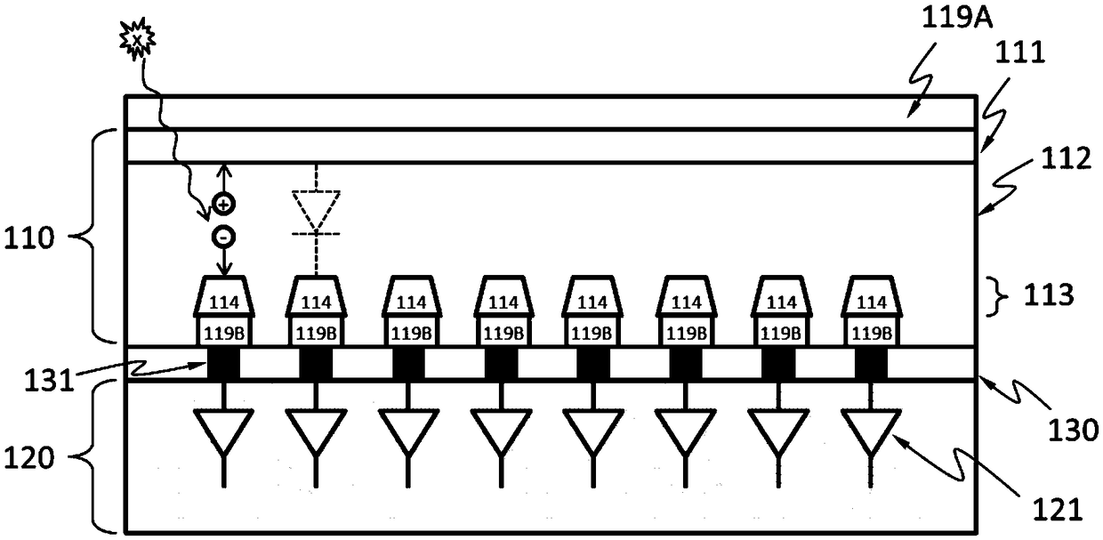
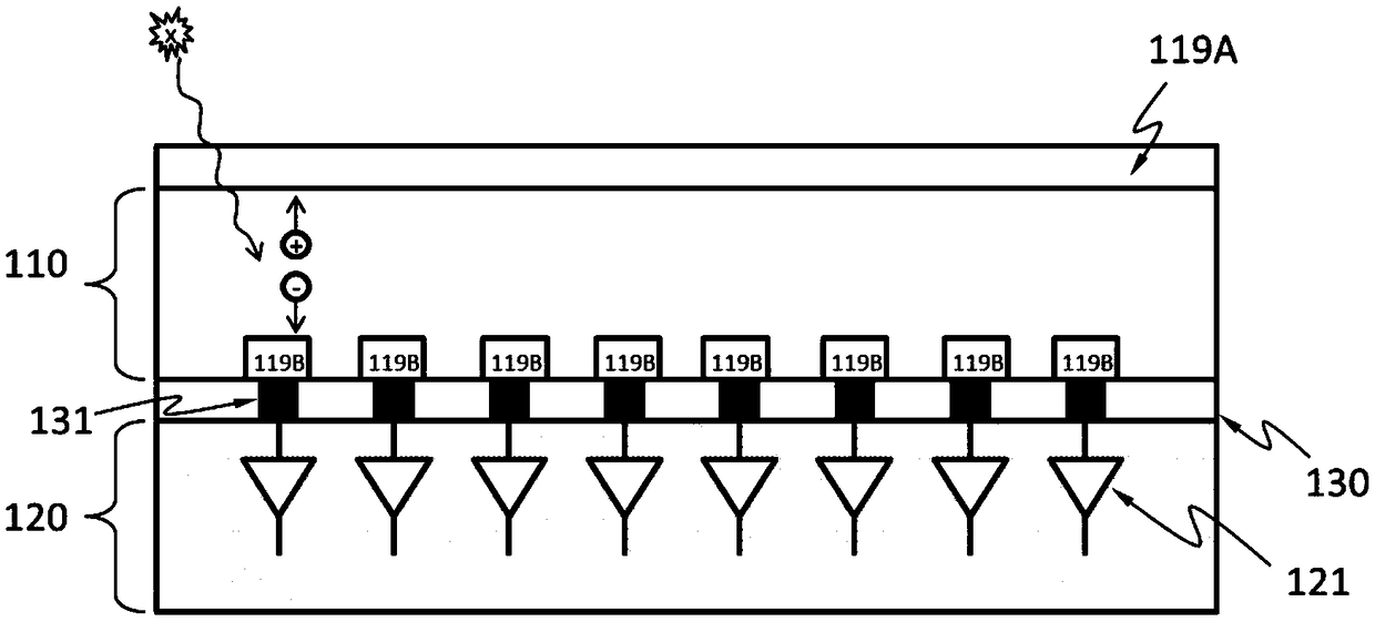
[0057] Figure 1A A cross-sectional view of the X-ray image detector 100 according to the embodiment is schematically shown. The detector 100 may include an X-ray absorbing layer 110 and an electronic layer 120 (for example, an ASIC) for processing or analyzing electrical signals generated in the X-ray absorbing layer 110 by incident X-rays. In an embodiment, detector 100 does not include a scintillator. The X-ray absorbing layer 110 may include semiconductor materials such as silicon, germanium, GaAs, CdTe, CdZnTe or combinations thereof. Semiconductors can have high mass attenuation coefficients for x-ray energies of interest.
[0058] as in Figure 1B As shown in the detailed cross-sectional view of the detector 100, according to an embodiment, the X-ray absorbing layer 110 may include one or more discrete regions 114 formed from the first doped region 111 and the second doped region 113 One or more diodes (for example, p-i-n or p-n). The second doped region 113 may be ...
PUM
 Abstract
Description
Claims
Application Information


