

Easy thermal erasing type liquid crystal membrane writing board and preparation method
A liquid crystal film and tablet technology, which is applied in the field of easily thermally erasable liquid crystal film tablet and its preparation, can solve problems such as inability to achieve partial erasing, reduce the risk of contact conduction, increase adhesion, and improve capacitive effect
- Summary
- Abstract
- Description
- Claims
- Application Information
AI Technical Summary
Problems solved by technology
Method used
Image

Examples
Embodiment 1
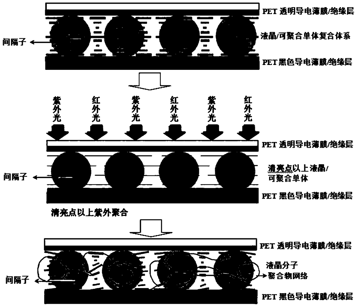
[0040] The easy-to-heat-erasable liquid crystal film writing board includes a PET (polyethylene terephthalate) transparent film, a liquid crystal thin layer, PET non-transparent black film coated with ITO on one side; insulating layer is coated on the conductive layer side of PET transparent film coated with ITO on one side and PET non-transparent black film coated with ITO on one side.
[0041] The thickness of the PET transparent film coated with ITO on one side and the non-transparent black film of PET coated with ITO on one side are both 188 microns; the thickness of the insulating layer is 2 microns; the thickness of the liquid crystal thin layer is 5 microns. Microns.
[0042] The insulating layer on one side of the conductive layer of the PET transparent film coated with ITO on one side is polyvinyl alcohol acrylate conformal paint.
[0043] The insulating layer on the conductive layer side of the non-transparent black film of PET coated with ITO on one side is polyvin...
Embodiment 2
[0070] The easy-to-heat-erasable liquid crystal film writing board includes a PET transparent film coated with ITO on one side, a liquid crystal thin layer, and a PET non-transparent black film coated with ITO on one side; The conductive layer of the PET transparent film and the PET non-transparent black film coated with ITO on one side are both coated with an insulating layer.
[0071] The thickness of the PET transparent film coated with ITO on one side and the non-transparent black film of PET coated with ITO on one side are both 188 microns; the thickness of the insulating layer is 2 microns; the thickness of the liquid crystal thin layer is 5 microns. Microns.
[0072] The insulating layer on one side of the conductive layer of the PET transparent film coated with ITO on one side is polyvinyl acetate.
[0073] The insulating layer on the conductive layer side of the non-transparent black film of PET coated with ITO on one side is polyvinyl acetate and spacers.
[0074] ...
Embodiment 3
[0099] The easy-to-heat-erasable liquid crystal film writing board includes a PET transparent film coated with ITO on one side, a liquid crystal thin layer, and a PET non-transparent black film coated with ITO on one side; The conductive layer of the PET transparent film and the PET non-transparent black film coated with ITO on one side are both coated with an insulating layer.
[0100] The thickness of the PET transparent film coated with ITO on one side and the non-transparent black film of PET coated with ITO on one side are both 188 microns; the thickness of the insulating layer is 2 microns; the thickness of the liquid crystal thin layer is 5 microns. Microns.
[0101] The insulating layer on one side of the conductive layer of the PET transparent film coated with ITO on one side is epoxy resin conformal paint.
[0102] The insulating layer on one side of the conductive layer of the non-transparent black film of PET coated with ITO is epoxy resin conformal paint and spac...
PUM
| Property | Measurement | Unit |
|---|---|---|
| Thickness | aaaaa | aaaaa |
| Thickness | aaaaa | aaaaa |
| Thickness | aaaaa | aaaaa |
Abstract
Description
Claims
Application Information