A method for preparing broadband reflective film material by nano-zinc oxide film diffusion method
A nano-zinc oxide, thin film diffusion technology, applied in chemical instruments and methods, liquid crystal materials, chemical industry and other directions, can solve problems such as limiting cholesteric liquid crystal, and achieve the effects of abundant sources, low material cost and simple system
- Summary
- Abstract
- Description
- Claims
- Application Information
AI Technical Summary
Problems solved by technology
Method used
Image
Examples
Embodiment 1
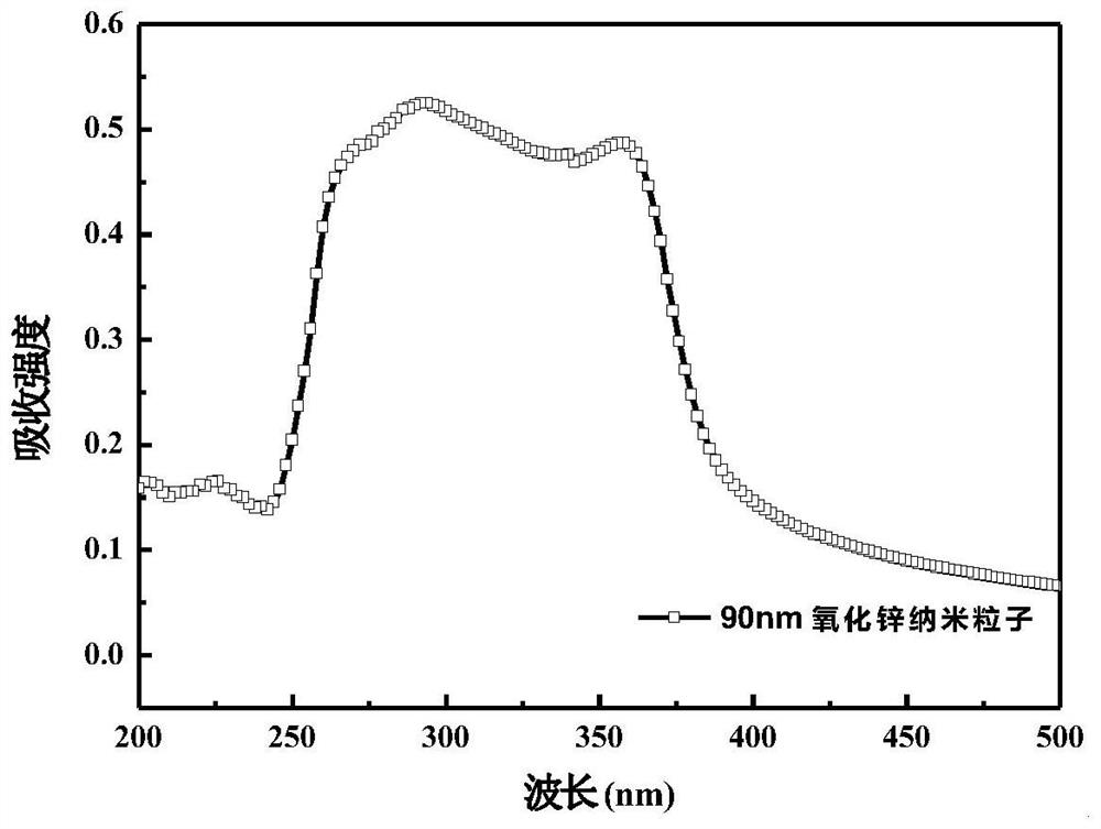
[0026] Fabrication of the liquid crystal cell: place the cleaned ITO (indium tin oxide) glass in a drying oven at 60° C. for 3 hours to dry. Get the nano-zinc oxide dispersion (≥30%, 90nm, solvent: 1,2-propylene glycol monomethyl ether acetate) and drop it on the ITO glass substrate, use a glue homogenizer to coat the ITO glass, the initial speed is 600r / min, spin The coating time is 6s, the high speed is 2000r / min, and the spin coating time is 30s. Afterwards, the glass substrate coated with the nano-zinc oxide film is heat-treated at a temperature of 60°C for 60 minutes to obtain a nano-zinc oxide film glass substrate. Combine the nano-zinc oxide film glass substrate with a piece of ITO glass substrate, use a PET film with a thickness of 55 μm as a spacer, seal the edges on both sides with glue, and leave the filling inlet, that is, prepare a nano-zinc oxide film on one side LCD box.
[0027] Mix the nematic liquid crystal SLC1717, the chiral compound R811, the polymerizabl...
Embodiment 2
[0037] Mix the nematic liquid crystal SLC1717, the chiral compound R811, the polymerizable monomer C6M and the photoinitiator Irg651 (benzil dimethyl ketal) in a mass ratio of 79.9:9.8:9.8:0.5, and use a siphon to The effect is poured into a liquid crystal cell containing a nano-zinc oxide film on one side.
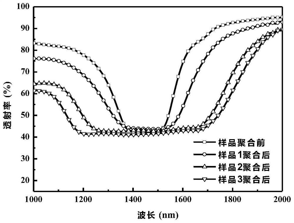
[0038] The sample compounded in Example 2 was poured into a liquid crystal cell containing a nano-zinc oxide film on one side. The thickness of the liquid crystal cell was 55 μm, and the liquid crystal cell was irradiated with ultraviolet light at 40° C. The degree is 0.8mW / cm 2 The 365nm ultraviolet light was irradiated for 60 minutes to obtain sample 2, so that the polymerizable monomers were cured and crosslinked to form a network, and the final polymer network cholesteric liquid crystal film was obtained. The reflection band of the film at room temperature was 1174nm-1738nm. The transmission spectrum of the sample prepared by the above method can be measured at room ...
Embodiment 3
[0040] Mix the nematic liquid crystal SLC1717, the chiral compound R811, the polymerizable monomer C6M and the photoinitiator Irg651 (benzil dimethyl ketal) in a mass ratio of 77.9:9.8:11.8:0.5, and use a siphon at room temperature to The effect is poured into a liquid crystal cell containing a nano-zinc oxide film on one side.
[0041] The sample compounded in Example 3 was poured into a liquid crystal cell containing a nano-zinc oxide film on one side. The thickness of the liquid crystal cell was 55 μm. The liquid crystal cell was irradiated with ultraviolet light at 40° C. 1.2mW / cm 2 The 365nm ultraviolet light was irradiated for 60 minutes to obtain sample 3, so that the polymerizable monomers were cured and crosslinked to form a network, and the final polymer network cholesteric liquid crystal film was obtained. The transmission spectrum of the sample can be measured at room temperature using an ultraviolet-visible-near-infrared spectrophotometer (Jasco V-570), and the r...
PUM
| Property | Measurement | Unit |
|---|---|---|
| thickness | aaaaa | aaaaa |
| particle diameter | aaaaa | aaaaa |
Abstract
Description
Claims
Application Information


