Ignition driving circuit

A driving circuit and resistor technology, applied in logic circuit interface devices, logic circuit connection/interface layout, electrical components, etc., can solve the problem that the gate source cannot maintain the conduction state at the moment of conduction, the ignition system malfunctions, and the saturation conduction state To avoid problems such as large pressure drop in the tube, to increase the anti-interference ability and solve the matching problem

Inactive Publication Date: 2018-11-02
XIAN MICROELECTRONICS TECH INST
View PDF12 Cites 3 Cited by
  • Summary
  • Abstract
  • Description
  • Claims
  • Application Information

AI Technical Summary

Problems solved by technology

[0005] 1. There is no isolation between the input and output stages, and the anti-interference ability is poor
[0006] There is no electrical isolation between the input and output stages of the traditional ignition drive circuit, and the output of the latter stage generally has a large current, which is easy to interfere with the small signal control part of the previous stage, resulting in misoperation of the ignition system
[0007] 2. If the output uses a high-power three-stage tube, the switching dynamic loss is relatively large
[0008] The traditional ignition circuit uses a high-power three-stage tube as the output. The saturated conduction state has a large pressure drop, low work efficiency, and rapid temperature rise. It is necessary to install a heat sink to ensure its normal operation.
[0009] 3. When the N-channel VDMOS tube is output, it cannot meet the requirements of the load ground terminal
[0010] The power supply of the optocoupler-isolated output terminal is the same power supply as the output power supply. If the N-channel VDMOS tube structure is used as the output, the load is grounded, and the voltage between the gate and the source at the moment of conduction will not be able to maintain its conduction state.

Method used


Image

  • Ignition driving circuit
  • Ignition driving circuit

Examples


Embodiment Construction

[0024] The present invention will be further described below in conjunction with the accompanying drawings and embodiments.

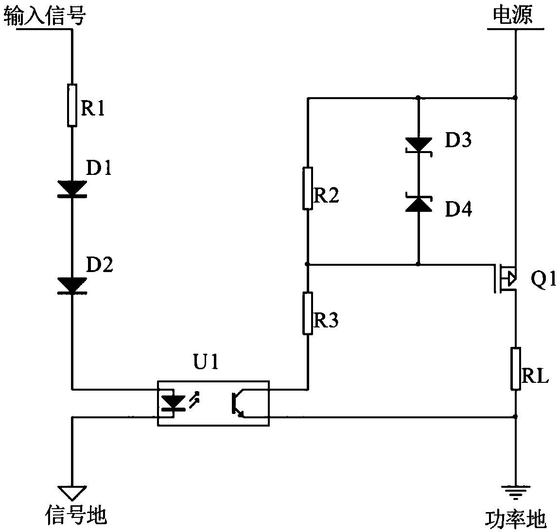
[0025] The principle block diagram of the ignition drive circuit of the present invention is as figure 1 shown. The input signal of the circuit passes through the resistor R1 to control the current flowing into the optocoupler. When the current is large enough, the light-emitting tube inside the optocoupler emits light, and the photosensitive tube of the optocoupler is controlled to conduct. The signal ground of the input terminal is separated from the ground wire of the isolated output to prevent interference signals from being transmitted to the rear stage through the ground wire.

[0026] figure 2 It is the schematic diagram of the ignition drive circuit. The circuit is mainly composed of an input drive part, an optocoupler isolation part, and a P-channel VDMOS tube output part. The OLI series optocoupler is used for electrical isolation between ...


PUM


Abstract

The invention provides an ignition driving circuit, which comprises an input end, a photocoupler U1 and a VDMOS tube Q1, wherein an input signal of the input end is connected in series with a diode D1and a diode D2 via a resistor R1 and then connected to the positive end of a light emitting tube of the photocoupler U1, and the negative terminal of the light emitting tube is connected with the signal ground; a power source is connected in series with the resistor R2 and the resistor R3 and is connected to a photosensitive tube collector of the photocoupler U1, and the emission electrode of thephotosensitive tube is connected with the power ground; meanwhile, the power supply is subjected to voltage division through the resistor R2 and the resistor R3 and drives the grid electrode of the VDMOS tube Q1, and two reverse voltage regulators D3 and D4 are connected in series between the grid electrode and the source electrode of Q1; and a load resistor RL is connected in series between thedrain electrode of the VDMOS tube Q1 and the power ground. The ignition driving circuit in the invention is directed to the specific use requirements of the ignition system and the situation of the load grounding end, considering the isolation between the front and rear stages to improve the anti-interference ability of the circuit and designing an ignition circuit and the like with small packagesize and strong driving capability.

Description

technical field [0001] The invention relates to the design technology of a semiconductor hybrid integrated circuit, in particular to an ignition drive control type hybrid integrated circuit. Background technique [0002] The traditional ignition circuit is a contact ignition system, which has large size, low reliability, and poor anti-interference ability. The ignition status is greatly affected by the speed and technical status of the contacts, and requires frequent maintenance and adjustment. Therefore, it is of great significance to design an ignition drive circuit with small size, high reliability and strong anti-interference ability. [0003] The characteristic of the ignition drive control system is that the ignition work is realized by controlling the output pulse large current of the rear stage through the small signal of the front stage. In order to prevent the circuit from overheating and reduce the power consumption of the circuit, high-power tubes with large dri...

Claims


Application Information

Patent Timeline
Patent Type & Authority Applications(China)
IPC IPC(8): H03K17/567H03K19/0175H02M1/092
CPCH02M1/092H03K17/567H03K19/017536H03K2217/0081
Inventor 苏斌黄华杨昊泽
Owner XIAN MICROELECTRONICS TECH INST
Why Eureka
Try Eureka