A device and method for detecting surface damage defects based on side-view camera shooting

A defect detection and surface damage technology, applied in the direction of optical testing flaws/defects, etc., can solve problems such as low detection accuracy and inability to automatically adjust, and achieve the effect of fewer light sources, improved accuracy, and reduced complexity and cost.

Active Publication Date: 2021-12-07
WUHAN JINGCE ELECTRONICS GRP CO LTD
View PDF0 Cites 0 Cited by
  • Summary
  • Abstract
  • Description
  • Claims
  • Application Information

AI Technical Summary

Problems solved by technology

[0008] Aiming at at least one defect or improvement requirement of the prior art, the present invention provides a surface damage defect detection device and method based on side-view camera photography, the purpose of which is to solve the defect detection accuracy of existing surface defect detection devices. High, unable to automatically adjust the position of the camera and light source according to the size of the display screen

Method used


Image

  • A device and method for detecting surface damage defects based on side-view camera shooting
  • A device and method for detecting surface damage defects based on side-view camera shooting
  • A device and method for detecting surface damage defects based on side-view camera shooting

Examples


Embodiment Construction

[0054] In order to make the object, technical solution and advantages of the present invention clearer, the present invention will be further described in detail below in conjunction with the accompanying drawings and embodiments. It should be understood that the specific embodiments described here are only used to explain the present invention, not to limit the present invention. In addition, the technical features involved in the various embodiments of the present invention described below can be combined with each other as long as they do not constitute a conflict with each other.

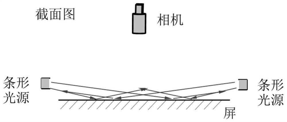
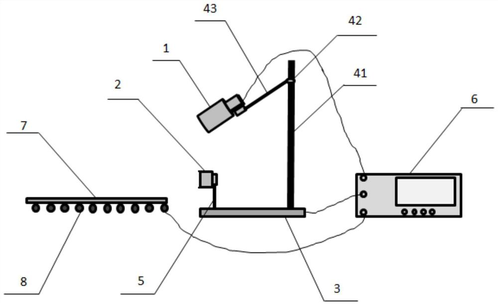
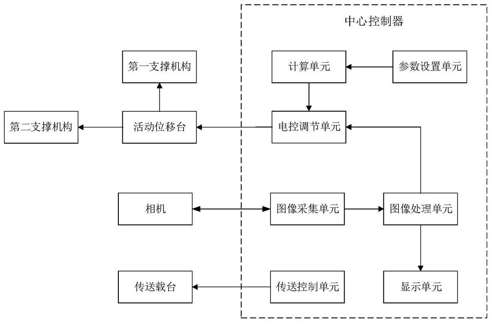
[0055] figure 2 It is a schematic structural diagram of a surface damage defect detection device and method based on a side-view camera photographed by an embodiment of the present invention; figure 2 As shown, the surface damage defect detection device includes a camera 1 (with a lens), a strip light source 2, a movable translation platform 3, a first support mechanism 4, a second support me...


PUM


Abstract

The invention belongs to the technical field of automatic defect detection of panels, and discloses a surface damage defect detection device and method based on shooting by a side-view camera, comprising a camera, a bar light source, a position adjustment mechanism and a central controller; the camera and the position adjustment The mechanism is connected with the central controller through a control cable; the strip light source and the camera are arranged on a position adjustment mechanism located on one side of the display screen to be tested; the camera and the strip light source are located on the same side of the display screen, and the camera and the display There is a set shooting angle between the screens; the invention adopts a strip light source as the lighting light source, and sets the shooting camera and the strip light source on the same side of the display screen, so as to avoid the uneven shooting picture of the camera caused by multiple light sources If the defect is imaged on the shooting screen of the camera with a higher contrast, the accuracy of defect detection can be improved.

Description

technical field [0001] The invention belongs to the technical field of automatic defect detection of panels, and more specifically relates to a surface damage defect detection device and method based on side-view camera photography. Background technique [0002] The production process of new display screens such as LCD / OLED includes nearly a hundred processes. Although most of the processes of the display screen are completed in a clean room, various defects such as cracks, scratches, and dirty surfaces are still inevitable. , air bubbles and surface particles, etc.; these defects will seriously affect the display performance of the display, so defect detection is required before leaving the factory; [0003] The current detection methods mostly use Automatic Optical Inspection (AOI), which uses optical imaging technology (usually using cameras and lenses) to obtain images of the target to be measured, and then passes through certain image processing algorithms to obtain ima...

Claims


Application Information

Patent Timeline
Patent Type & Authority Patents(China)
IPC IPC(8): G01N21/95
CPCG01N21/95
Inventor 洪志坤张胜森欧昌东郑增强
Owner WUHAN JINGCE ELECTRONICS GRP CO LTD
Why Eureka
Try Eureka