Supercharge Your Innovation With Domain-Expert AI Agents!

Signal combining circuit, gate driving unit, gate driving circuit and display device

一种栅极驱动、信号的技术,应用在信号合并电路,栅极驱动单元,栅极驱动电路和显示装置领域,能够解决无法适用外部补偿、栅极驱动芯片尺寸大、不利窄边框实现等问题

Active Publication Date: 2018-11-06
BOE TECH GRP CO LTD +1
View PDF9 Cites 6 Cited by
  • Summary
  • Abstract
  • Description
  • Claims
  • Application Information

AI Technical Summary

Problems solved by technology

Among them, if the gate drive unit is implemented by using a gate drive chip, although it can output double pulse signals, it is not conducive to the realization of a narrow frame due to the large size of the gate drive chip; if the gate drive unit uses a gate The driver circuit (Gate Driver on Array, referred to as GOA), although it can achieve a narrow frame design, but because each shift register can only output a single pulse signal within one frame time, it is not suitable for external compensation

Method used


Image

  • Signal combining circuit, gate driving unit, gate driving circuit and display device
  • Signal combining circuit, gate driving unit, gate driving circuit and display device
  • Signal combining circuit, gate driving unit, gate driving circuit and display device

Examples


Embodiment Construction

[0052] In order for those skilled in the art to better understand the technical solution of the present invention, a signal combination circuit, a gate drive unit, a gate drive circuit and a display device provided by the present invention will be described in detail below with reference to the accompanying drawings.

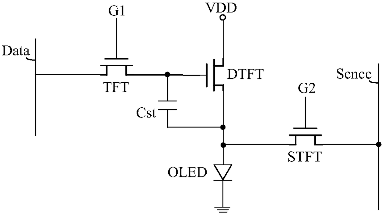
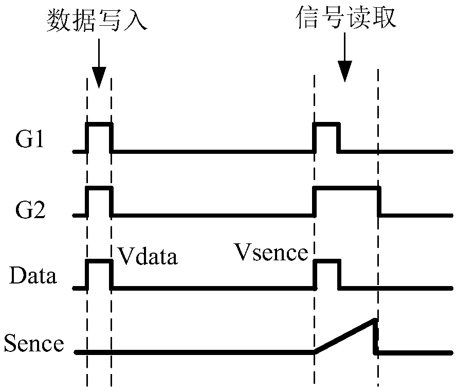
[0053] figure 1 It is a schematic circuit structure diagram of a pixel circuit in an organic light emitting diode display panel, figure 2 for figure 1 The working timing diagram of the shown pixel circuit, such as figure 1 and figure 2 As shown, the pixel circuit includes a switching transistor TFT, a driving transistor DTFT, a sensing transistor STFT and a capacitor Cst. When only external compensation is required for the pixel circuit, the pixel circuit includes at least the following two stages in the working process: a data writing stage and a sensing stage (including a signal reading process).

[0054] In the data writing phase, the data voltage Vdata...


PUM


Abstract

The invention discloses a signal combining circuit, a gate driving unit, a gate driving circuit and a display device. The signal combining circuit includes a first active level output circuit, a firstinactive level output circuit and a node voltage control circuit, wherein the first active level output circuit is used for writing an active level voltage to a driving signal output end when a signal supplied by a first signal output end or a second signal output end is in an active level state, and the first inactive level output circuit is used for writing an inactive level voltage to the driving signal output end when signals supplied by the first signal output end and the second signal output end are both in an inactive level state. The technical scheme of the invention can realize the combination of monopulse signals output by two shifting registers, thereby outputting a double-pulse driving signal to meet a requirement of sensing the driving of a transistor; and in addition, the technical scheme is based on a GOA circuit, which is beneficial to the narrow-frame design of an OLED display panel.

Description

technical field [0001] The present invention relates to the field of display technology, in particular to a signal combination circuit, a gate drive unit, a gate drive circuit and a display device. Background technique [0002] In the process of driving the OLED in the organic light-emitting diode (Organic Light-Emitting Diode, referred to as OLED) display panel, due to the performance difference of each driving transistor or OLED (difference caused by process, difference caused by aging), it will cause The display brightness is not uniform, so the performance of the drive transistor or OLED needs to be compensated. [0003] Among them, external compensation is a common compensation method. Specifically, external compensation refers to extracting the current at the drive transistor or OLED through the sensing circuit, and after reading out the electrical signal, implements a more complex algorithm with the help of an external integrated circuit chip to compensate for the no...

Claims


Application Information

Patent Timeline
Patent Type & Authority Applications(China)
IPC IPC(8): G09G3/3266
CPCG09G3/3266G09G2310/0286G09G2300/0819G09G2310/08G09G2320/029G09G2320/045G09G3/3258G09G2300/0408G09G2310/0243
Inventor 袁志东李永谦袁粲何敏
Owner BOE TECH GRP CO LTD
Features
  • R&D
  • Intellectual Property
  • Life Sciences
  • Materials
  • Tech Scout
  • Unparalleled Data Quality
  • Higher Quality Content
  • 60% Fewer Hallucinations
Learn More