Multi-chip wiring substrate, wiring substrate

A technology of wiring substrates and multi-pieces, which is applied in the field of manufacturing multi-pieces wiring substrates, and can solve problems such as small width of dividing grooves

Active Publication Date: 2021-11-30
KYOCERA CORP
View PDF5 Cites 0 Cited by
  • Summary
  • Abstract
  • Description
  • Claims
  • Application Information

AI Technical Summary

Problems solved by technology

That is, by forming through-holes for the positional deviation of the dividing grooves in the upper and lower surfaces, it is possible to make a multi-piece wiring board that is not easily affected by the positional deviation of the dividing grooves. In the case of a wiring board on which through holes are formed, in the processing of the dividing grooves by laser, the width of the dividing grooves is smaller than that of the conventional dividing grooves formed mechanically by using a mold or the like. Compared with a mother board in a wiring board region with a through-hole, a mother board in which a wiring board region without a through-hole is arranged has the problem that, when the position of the dividing groove is shifted, etc., the wiring board region Difficult to segment the corners of

Method used


Image

  • Multi-chip wiring substrate, wiring substrate
  • Multi-chip wiring substrate, wiring substrate
  • Multi-chip wiring substrate, wiring substrate

Examples


Embodiment Construction

[0025] The manufacturing method of the multi-connective wiring substrate, a wiring substrate, a multi-connective wiring substrate of the present invention will be described with reference to the drawings.

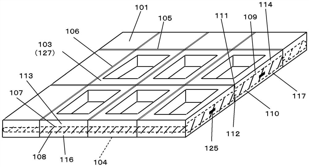
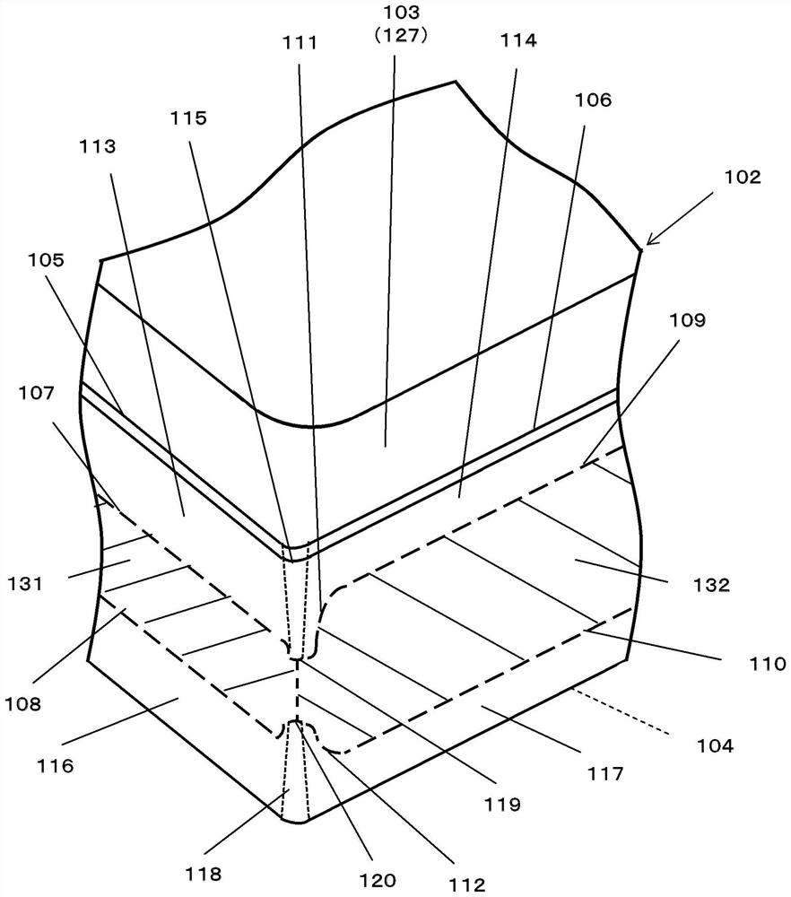
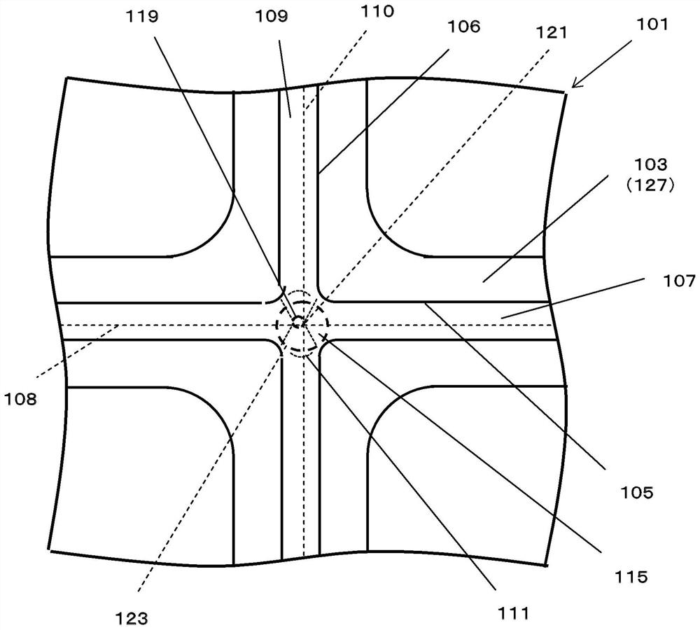
[0026] exist Figure 1 ~ 8 In the middle, 101 is the mother-based plate, 102 is a wiring substrate, 103 is the first main surface, 104 is the second main surface, 105 is the side of the one, 106 is the other side, 107 is the first split slot, 108 is the second The split groove, 109 is a third split groove, 110 is a fourth-cut slot, 111 is a first curvature, 112 is a second curved portion, 114 is the first side, 115 is the first curved surface, 116 Is the third side, 117 is the fourth side, 118 is the second curved surface, 119 is the first bottom, 120 is the second bottom, 121 is the first intersection, 122 is the second intersection, 123 is the first false circle, 124 is a second false circle, 125 is a connecting wiring conductor, 126 is laser, 127 is a frame-shaped metal layer. ...


PUM


Abstract

The multi-piece wiring substrate includes: a mother substrate having a first main surface and a second main surface opposite to the first main surface, and a plurality of wiring substrate regions are arranged, the mother substrate includes: a division groove along the wiring substrate region The boundary of the boundary is set on the first main surface and the second main surface, and the dividing groove has: the first dividing groove, which is arranged on the first main surface of one side of the wiring substrate region; the second dividing groove, which is opposite to the first dividing groove Provided on the second main surface; the third dividing groove is provided on the first main surface of the other side of the wiring substrate region; and the fourth dividing groove is provided on the second main surface opposite to the third dividing groove, and the first The depth of the division groove and the depth of the second division groove are set larger than the depth of the third division groove and the depth of the fourth division groove, and the depth of the third division groove is gradually increased toward the corner of the wiring board region. a curved portion, and has a second curved portion in which the depth of the fourth dividing groove gradually increases toward the corner of the wiring substrate region.

Description

Technical field [0001] The present invention relates to a multi-link substrate, a wiring substrate, a wiring substrate, a wiring substrate, and a multi-linking substrate, a plurality of wiring substrates, a plurality of wiring substrates, a plurality of wiring substrate regions having a mounting portion having an electronic component as a longitudinally arranged. Background technique [0002] Incidentally, a multi-connective wiring substrate having a plurality of wiring substrate regions is known as the mother substrate is known. The split groove is formed in the main surface of the mother substrate or the like along the boundary of the wiring substrate region. By applying a bending stress by sandwiching the split groove, the mother substrate is broken, thereby being divided into a wiring substrate. The split groove is formed, for example, by using a cutting knife or the like by a cutting knife or the like by a cutting cutter along the outer circumference of the outer surface of ...

Claims


Application Information

Patent Timeline
Patent Type & Authority Patents(China)
IPC IPC(8): H05K1/02H01L23/12H05K3/00
CPCH01L21/4846H01L23/13H01L23/498H05K3/0052H05K3/4629H05K2201/0909H05K3/0026H05K3/0097H01L23/544H03B5/326H03H3/02H03H3/08H03H9/02897H03H9/058H03H9/19H05K1/02H05K1/0284H05K1/0298H05K1/03H05K1/119H05K3/00H05K3/0029H05K2203/107
Inventor 鬼塚善友
Owner KYOCERA CORP
Why Eureka
Try Eureka