Devices and methods for calibrating and operating a snapback clamp circuit

a technology of snapback clamping and devices, applied in the direction of electric variable regulation, process and machine control, instruments, etc., can solve the problems of damage to electronic devices that utilize integrated circuits, damage to electronic devices that damage electronic devices, damage to electronic devices that alter the operation of electronic devices, etc., and achieve the effect of discharging curren

Active Publication Date: 2015-11-10
QUALCOMM INC
View PDF23 Cites 0 Cited by
  • Summary
  • Abstract
  • Description
  • Claims
  • Application Information

AI Technical Summary

Benefits of technology

[0005]A snapback clamp circuit in accordance with at least one embodiment of the present disclosure includes a snapback clamp circuit having a trigger voltage level that may be calibrated. Operation of the snapback clamp circuit may advantageously incorporate a fast response time associated with snapback clamp circuits while clamping in response to a trigger voltage level that can be calibrated (e.g., lowered) to within a suitable range (e.g., low enough to not damage certain circuit components during ESD events), thus enabling both supply glitch suppression and ESD protection. For example, the trigger voltage level may be calibrated based on a selected body-to-ground resistance associated with the snapback clamp circuit, based on a gate-to-source voltage applied at the snapback clamp circuit, or a combination thereof. In a particular illustrative embodiment, the snapback clamp circuit is included within an integrated circuit and the trigger voltage level is calibrated based on supply glitches caused by off-chip trace inductances associated with a supply voltage that supplies the integrated circuit (or a portion thereof), as explained further below.
[0006]To illustrate, a device may include an integrated circuit having a class-D amplifier that drives a speaker. The class-D amplifier may be configured to generate a high-frequency square wave signal (e.g., a 600 kilohertz (kHz) square wave signal that encodes an audio signal). The class-D amplifier may be “switched” on and off quickly to generate the square wave signal. Faster switching may be associated with better performance (e.g., better signal resolution, less harmonic distortion, or a combination thereof). However, rapidly switching transistors on and off to generate the high-frequency square wave signal may cause spikes or “glitches” in the amplifier power supply, such as by causing off-chip trace inductances to output a voltage in response to changes in the amount of current drawn by the class-D amplifier. The supply voltage glitches can cause soft damage (e.g., decreased performance, such as increased harmonic distortion) or hard damage (e.g., hardware damage, such as damage to low-power components not designed to operate in connection with supply glitches) to the device. In at least one embodiment, a programmable snapback clamp circuit may be calibrated (e.g., by calibrating a trigger voltage level of the snapback clamp circuit) based on the trace inductances to suppress the glitches in the amplifier power supply, as explained further below.
[0012]In another particular embodiment, an integrated circuit includes a snapback clamp circuit having a trigger voltage level. The trigger voltage level is determined based on a programmed bias device of the snapback clamp circuit, a programmed body-to-ground resistance of the snapback clamp circuit, or a combination thereof, The snapback clamp circuit is configured to clamp a supply voltage in response to the supply voltage exceeding the trigger voltage level during an electrostatic discharge (ESD) event. The snapback clamp circuit enables glitch-suppression and ESD protection of the integrated circuit.
[0013]In another particular embodiment, a method of operating an integrated circuit is disclosed. The method includes, in response to a supply voltage exceeding a trigger voltage level during an electrostatic discharge (ESD) event, clamping the supply voltage by a snapback clamp circuit of the integrated circuit. The trigger voltage level is determined responsive to a programmed bias device of the snapback clamp circuit, a programmed body-to-ground resistance of the snapback clamp circuit, or a combination thereof. The snapback clamp circuit enables glitch suppression and ESD protection of the integrated circuit.

Problems solved by technology

Fluctuations in a supply voltage associated with an electronic device may damage or alter operation of the electronic device.
For example, “glitches” associated with the supply voltage may cause “spikes” in the supply voltage, which may potentially damage components of the electronic device, such as an integrated circuit.
ESD can severely alter operation of the integrated circuit or cause damage to the integrated circuit (e.g., by damaging gate oxide layers of transistors of the integrated circuit), thereby damaging the electronic device that utilizes the integrated circuit.
However, big FET clamp circuits may be associated with a slow response time and therefore may not be suitable for supply glitch protection in certain applications.
The snapback clamp circuit may not be suitable for electrostatic discharge (ESD) protection in some applications, since certain circuit components may not be designed to withstand a relatively large holding voltage associated with the snapback clamp circuit (e.g., a voltage to which the snapback clamp circuit “snaps back” during clamping operation).
However, rapidly switching transistors on and off to generate the high-frequency square wave signal may cause spikes or “glitches” in the amplifier power supply, such as by causing off-chip trace inductances to output a voltage in response to changes in the amount of current drawn by the class-D amplifier.
The supply voltage glitches can cause soft damage (e.g., decreased performance, such as increased harmonic distortion) or hard damage (e.g., hardware damage, such as damage to low-power components not designed to operate in connection with supply glitches) to the device.

Method used


Image

  • Devices and methods for calibrating and operating a snapback clamp circuit
  • Devices and methods for calibrating and operating a snapback clamp circuit
  • Devices and methods for calibrating and operating a snapback clamp circuit

Examples


Embodiment Construction

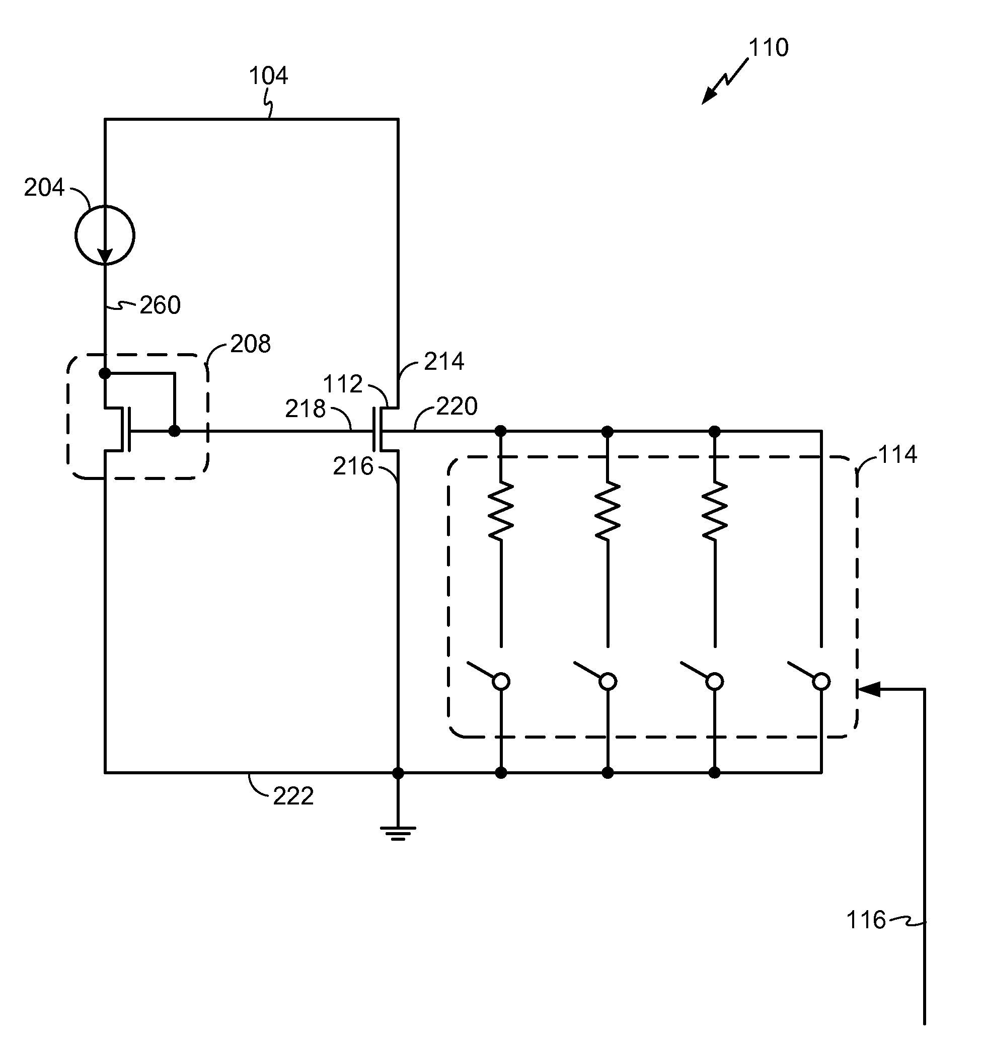
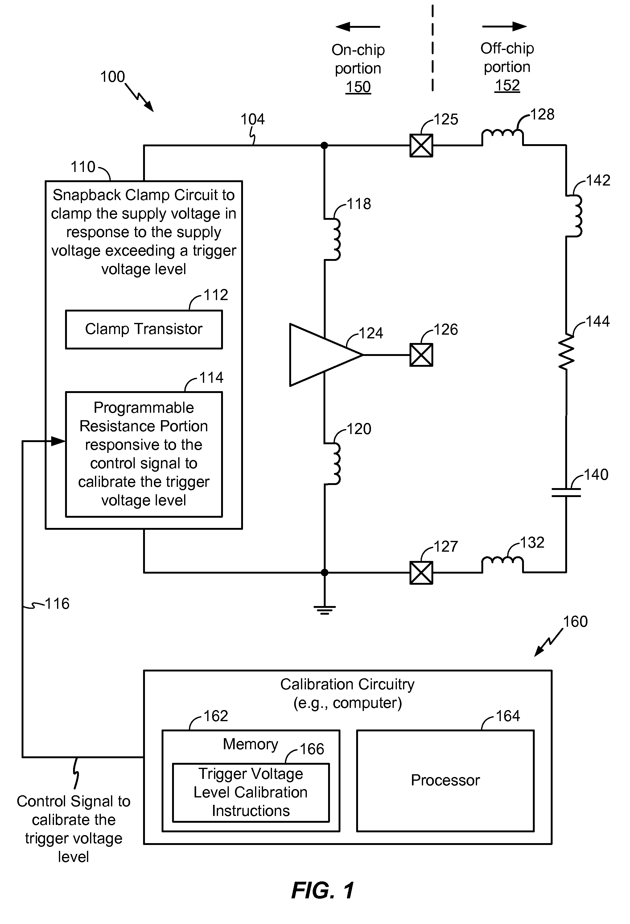
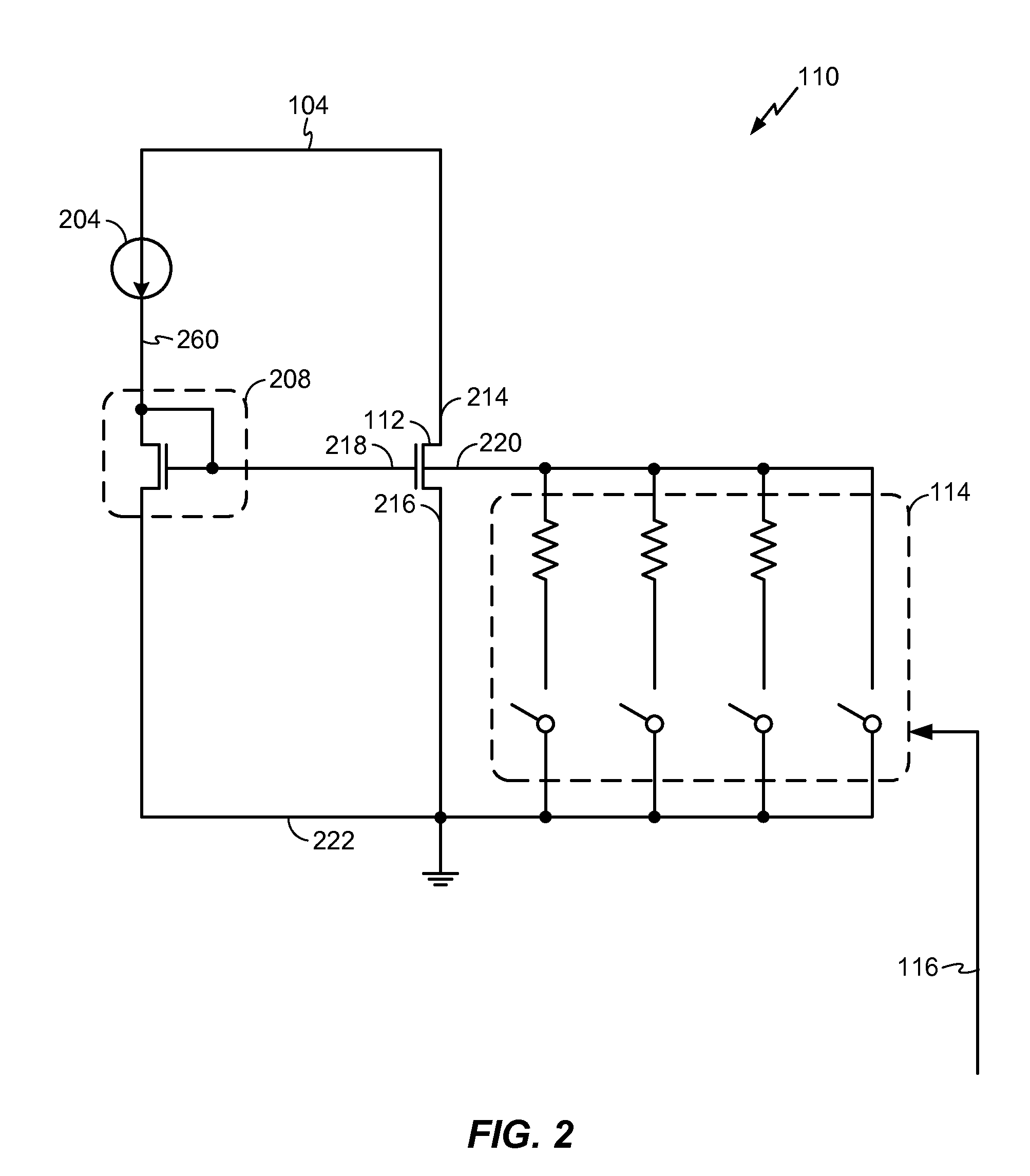
[0025]FIG. 1 depicts a particular illustrative embodiment of a system that includes a device 100 and calibration circuitry 160 (e.g., a computer). The calibration circuitry 160 includes a memory 162 (e.g., a computer-readable memory) coupled to a processor 164. The memory 162 may store trigger voltage level calibration instructions 166 executable by the processor 164 to generate a control signal 116, as explained further below. As used herein, a memory, such as the memory 162, may include a random access memory (RAM), flash memory, read-only memory (ROM), programmable read-only memory (PROM), erasable programmable read-only memory (EPROM), electrically erasable programmable read-only memory (EEPROM), registers, hard disk, a removable disk, or any other form of non-transitory storage medium.

[0026]The device 100 may include an on-chip portion 150 (e.g., an integrated circuit) and an off-chip portion 152 (e.g., power supply circuitry associated with the device 100). The on-chip portion...


PUM


Abstract

A device includes a snapback clamp circuit configured to clamp a supply voltage in response to the supply voltage exceeding a trigger voltage level. In at least one embodiment, the snapback clamp circuit includes a clamp transistor and a programmable resistance portion that is responsive to a control signal to calibrate the trigger voltage level. Alternatively or in addition, the snapback clamp circuit may include a programmable bias device configured to calibrate the trigger voltage level by biasing a gate terminal of the clamp transistor. In another particular embodiment, a method of calibrating a snapback clamp circuit is disclosed. In another particular embodiment, a method of operating an integrated circuit is disclosed.

Description

I. FIELD[0001]The present disclosure is generally related to electronic devices and more particularly to electronic devices that include snapback clamp circuits.II. DESCRIPTION OF RELATED ART[0002]Advances in technology have resulted in smaller and more powerful electronic devices. For example, there currently exist a variety of portable electronic devices, including portable wireless telephones, personal digital assistants (PDAs), and paging devices, which may be small, lightweight, and easily carried by users. Certain electronic devices, such as cellular telephones and wireless Internet Protocol (IP) telephones, can communicate voice and data packets over wireless networks. Further, many such electronic devices include other types of devices that are incorporated therein. For example, a wireless telephone can also include a digital still camera, a digital video camera, a digital recorder, and an audio file player. Also, wireless telephones can process executable instructions, incl...

Claims


Application Information

Patent Timeline
Patent Type & Authority Patents(United States)
IPC IPC(8): H02H9/00H02H9/04H01L27/06H01L27/02G05F1/10H02H3/00
CPCG05F1/10H01L27/0274H01L27/0277H01L27/0629H02H9/041H02H9/046H02H3/006
Inventor SRIVASTAVA, ANKITSIENKO, MATTHEW DAVIDWORLEY, EUGENE ROBERT
Owner QUALCOMM INC
Why Eureka
Try Eureka