QLED device, display device and manufacturing method thereof
A device and mesoporous material technology, applied in the field of QLED devices, display devices and their preparation, can solve the problems of low luminous efficiency, difficult to effectively control the thickness of the device, and high production cost, and achieve the improvement of luminous efficiency, reduction of control costs, and simple method. easy-to-control effects
- Summary
- Abstract
- Description
- Claims
- Application Information
AI Technical Summary
Problems solved by technology
Method used
Image

Examples
Embodiment Construction
[0018] In order to make the object, technical solution and advantages of the present invention clearer, the present invention will be further described in detail below in conjunction with the accompanying drawings and embodiments. It should be understood that the specific embodiments described here are only used to explain the present invention, not to limit the present invention.
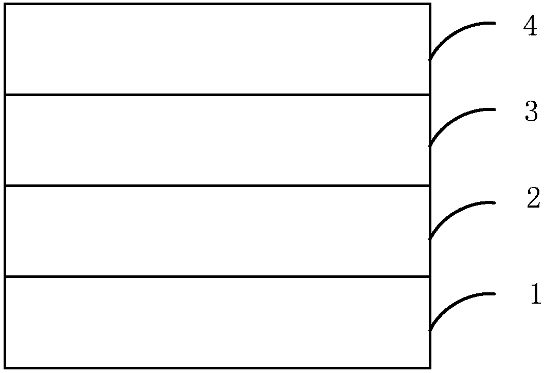
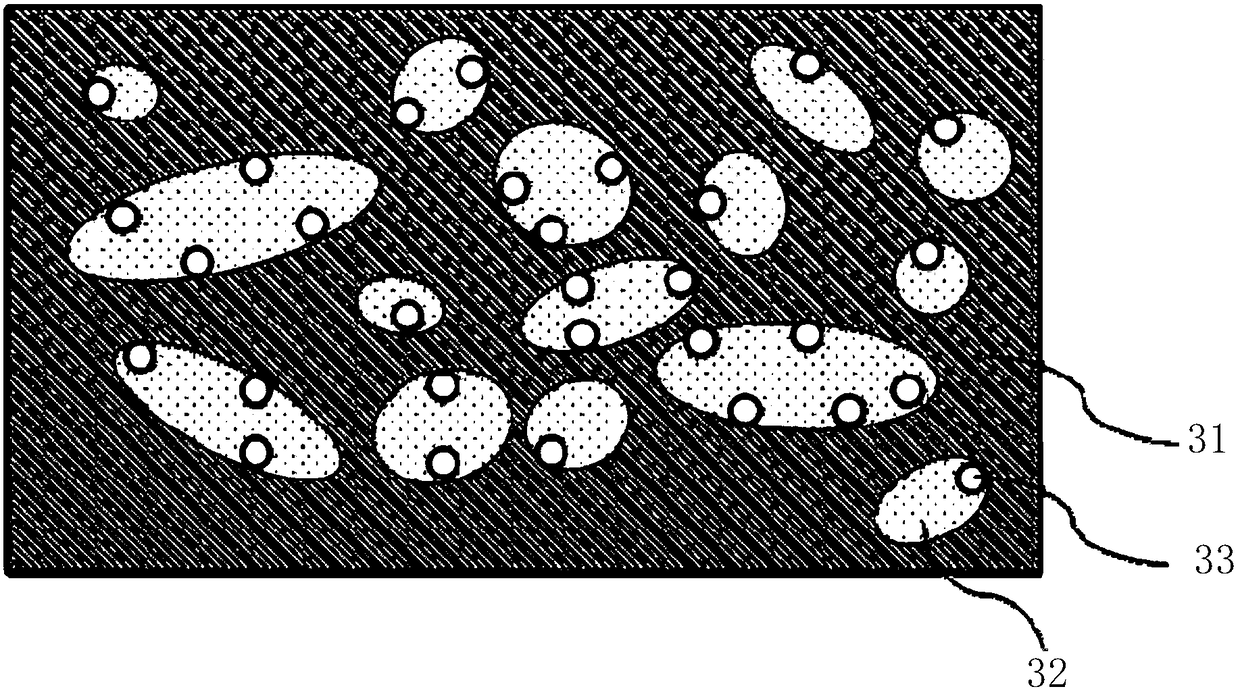
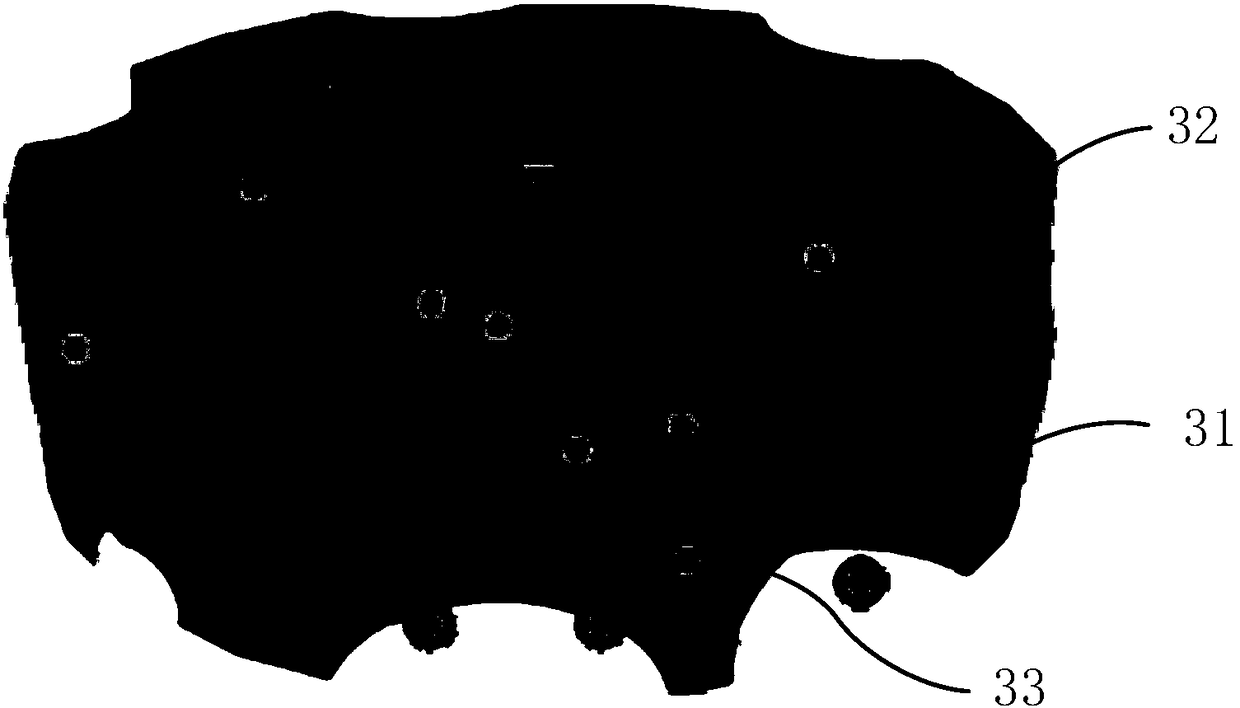
[0019] combine Figure 1-Figure 3 , the embodiment of the present invention provides a QLED, such as figure 1 As shown, it includes a substrate 1, a bottom electrode 2, a quantum dot luminescent layer 3 and a top electrode 4 arranged in sequence. The quantum dot luminescent layer 3 is composed of a mesoporous material 31 and an electrolyte 32 filled in the pores of the mesoporous material 31 and luminescent quantum dots. 33 components (see figure 2 or image 3 ), wherein, the conductivity of the electrolyte 32 ≥ 0.01scm -1 .
[0020] In the embodiment of the present invention, the QLED device...
PUM
| Property | Measurement | Unit |
|---|---|---|
| Conductivity | aaaaa | aaaaa |
| Conductivity | aaaaa | aaaaa |
| Linearity | aaaaa | aaaaa |
Abstract
Description
Claims
Application Information
 - Generate Ideas
- Intellectual Property
- Life Sciences
- Materials
- Tech Scout
- Unparalleled Data Quality
- Higher Quality Content
- 60% Fewer Hallucinations
Browse by: Latest US Patents, China's latest patents, Technical Efficacy Thesaurus, Application Domain, Technology Topic, Popular Technical Reports.
© 2025 PatSnap. All rights reserved.Legal|Privacy policy|Modern Slavery Act Transparency Statement|Sitemap|About US| Contact US: help@patsnap.com