Device and process method for preparing base material and inner surface metallization circuit based on 3D printing integration

A 3D printing and 3D printer technology, applied in printed circuits, printed circuit manufacturing, electrical components, etc., can solve problems such as inability to prepare electronic circuits, and achieve the effects of simplifying the manufacturing process, reducing manufacturing costs, and shortening the manufacturing cycle.

Active Publication Date: 2021-07-16
西安瑞特三维科技有限公司
View PDF4 Cites 1 Cited by
  • Summary
  • Abstract
  • Description
  • Claims
  • Application Information

AI Technical Summary

Problems solved by technology

[0005] The existing surface metal circuit preparation process mainly relies on film sticking and transfer printing methods. For the inner wall of irregular curved surface, due to the influence of cavity size and structural interference, it is impossible to use traditional technology to complete the electronic circuit on the inner wall. preparation of

Method used


Image

  • Device and process method for preparing base material and inner surface metallization circuit based on 3D printing integration
  • Device and process method for preparing base material and inner surface metallization circuit based on 3D printing integration
  • Device and process method for preparing base material and inner surface metallization circuit based on 3D printing integration

Examples


Embodiment Construction

[0037] Embodiments of the present invention are described in detail below, and the embodiments are exemplary and intended to explain the present invention, but should not be construed as limiting the present invention.

[0038] Basic principle of the present invention is:

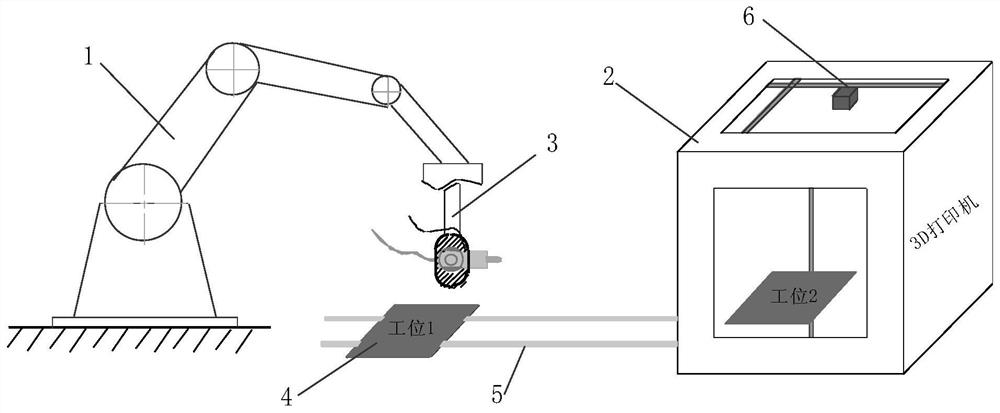
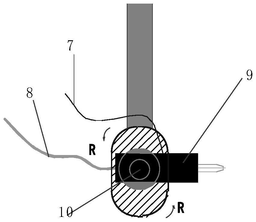
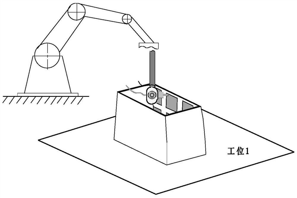
[0039] A 3D printer with three-axis movement is configured with a specific print head such as an inkjet or a melt extrusion head to print and form the base material. After setting a pause action when printing at a certain height, the printing platform is moved from the station through the slide rail. 2 Move to station 1. At this station, the mechanical arm system is used to extend the part of the device with the inkjet printing head into the inner cavity of the printed substrate (if the inner cavity opening is small, only rotate to control the inkjet head to adjust the angle), by controlling the rotation device Adjust the angle of the print head, start the printing action, and print the conductive paste on...


PUM


Abstract

The present invention provides a device and a process method for the integrated preparation of a substrate and an inner surface metallization circuit based on 3D printing. The device includes a robotic arm system, a 3D printer and a slide rail system. The principle is based on a 3D printer and uses an inkjet print head. Or melt extrusion head to print the structure of the antenna base material, in the process of printing the antenna base material, use the slide rail to switch the printing platform as a whole. Extend into the cavity of the formed substrate frame, control the printing nozzle to adjust to the normal direction to the inner surface of the substrate frame, and then turn on the printing function, and print the designed metal circuit pattern on the inner surface of the formed substrate according to the established trajectory. , After the printing of the graphics is completed, the printing platform is switched to the second station through the slide rail, and the printing of the substrate model is resumed. After that, the cyclic printing of the two processes is carried out to finally complete the integrated molding of the inner surface circuit structure. The invention can realize the rapid manufacture of conformal antennas, inner wall curved circuit patterns and the like.

Description

technical field [0001] The invention relates to the technical field of preparation of a metallized circuit substrate with an inner surface, in particular to a device and a process method for the integrated preparation of a substrate and a metallized circuit on an inner surface based on 3D printing. Background technique [0002] In view of the stealth and lightweight requirements of the missile seeker in the future, the antenna or stealth structure will be oriented to conformal design, and it is proposed that the metal graphics will be directly arranged inside the seeker radome, and the functions of the antenna and the radome will be compounded. Requirements to reduce the original antenna carrier to achieve the purpose of weight reduction. Make the seeker radome break through the function of the original structural parts, and make it have functional features. [0003] During the design process of the antenna and stealth structure, considering the heat generated by the fricti...

Claims


Application Information

Patent Timeline
Patent Type & Authority Patents(China)
IPC IPC(8): H05K3/12
CPCH05K3/125
Inventor 李超尹恩怀
Owner 西安瑞特三维科技有限公司
Why Eureka
Try Eureka