Scheduling optimization method and device in semiconductor production line CPS environment

A production line scheduling and optimization device technology, applied in control/adjustment systems, comprehensive factory control, instruments, etc., can solve the problems of scarcity of CPS environment scheduling optimization applications, blank research results, etc., to achieve frequent and efficient interaction, and improve calculation accuracy , the effect of reducing information delay

Inactive Publication Date: 2018-11-16
TONGJI UNIV
View PDF9 Cites 27 Cited by
  • Summary
  • Abstract
  • Description
  • Claims
  • Application Information

AI Technical Summary

Problems solved by technology

[0014] To sum up, in the current industrial production, the construction of CPS environment and the application of scheduling optimization in it are relatively scarce, especially in the field of production line scheduling for more complex semiconductor manufacturing systems, and its research results are still blank

Method used


Image

  • Scheduling optimization method and device in semiconductor production line CPS environment
  • Scheduling optimization method and device in semiconductor production line CPS environment
  • Scheduling optimization method and device in semiconductor production line CPS environment

Examples


Embodiment

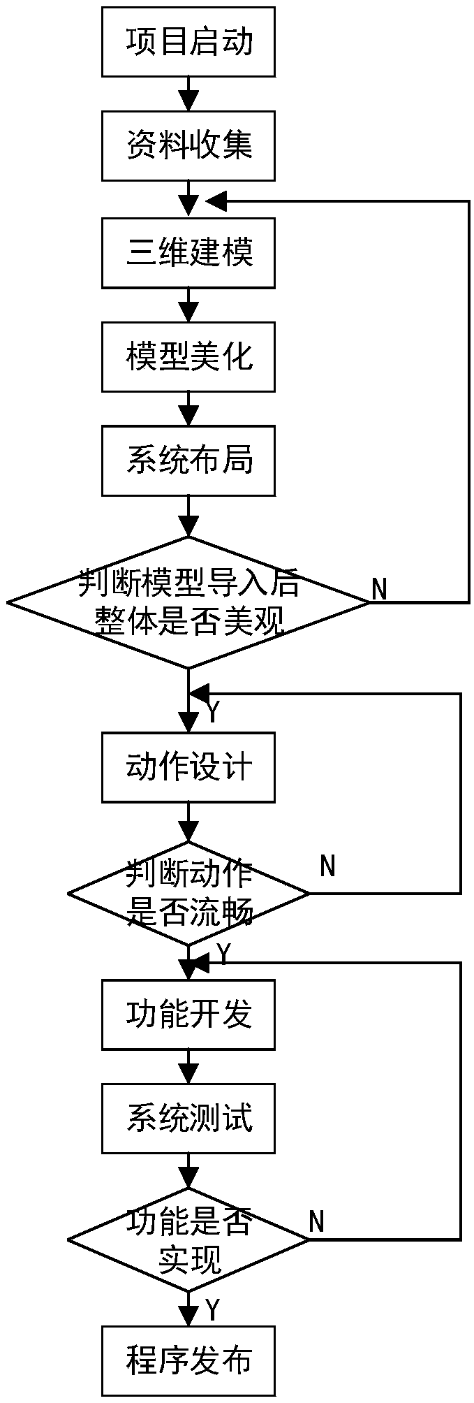
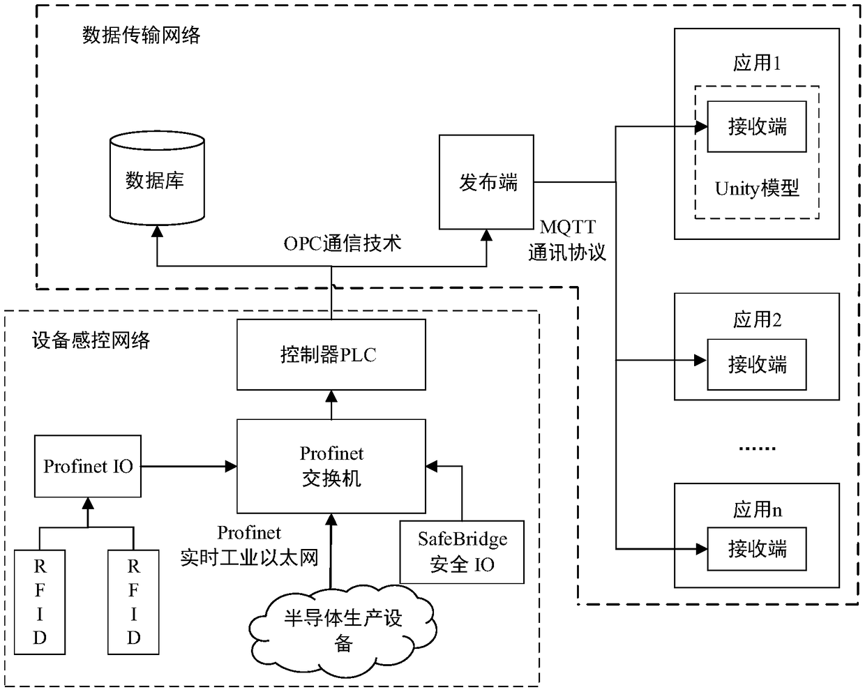
[0108] This embodiment uses python to realize the calculation logic of the designed scheduling method, and uses C# language to program the window interface, call the designed calculation model, integrate the scheduling module program with the CPS environment, and realize real-time scheduling in the semiconductor production process with control.

[0109] This embodiment is implemented in a smart manufacturing demonstration unit based on a semiconductor Minifab production line. The dispatching device of this embodiment realizes the simulation of the actual production process of the semiconductor MiniFab production line through technologies such as PROFINET, SafetyBridge, and RFID. The demonstration unit has one simulated lithography device, two simulated diffusion devices and two simulated ion implantation devices. In addition, the unit also includes a simulated storage location, which is composed of a raw material area and a finished product area, responsible for storing raw m...


PUM


Abstract

The invention relates to a scheduling optimization method and device in a semiconductor production line CPS environment, and the method specifically comprises the steps: constructing a semiconductor production line CPS environment for scheduling; sensing various types of sudden disturbances of a semiconductor production line in a production process; and performing the re-scheduling based on the dynamic information of the production line during the occurrence of the sudden disturbances. The device comprises a communication module which achieves the communication with an actual production line;a CPS environment constructing module which is used for constructing a digitalized three-dimensional model; a scheduling optimization design module which is used for sensing the production informationin real time, triggering the re-scheduling when the production information changes, generating a new production line scheduling scheme according to the dynamic information of the production line, andachieving the re-scheduling. Compared with the prior art, the method and device have the advantages that the method and device can be used for the semiconductor production line and other complex manufacturing systems, are high in timeliness, and are good in scheduling effect.

Description

technical field [0001] The invention relates to a semiconductor production line scheduling optimization technology, in particular to a scheduling optimization method and device in a semiconductor production line CPS environment. Background technique [0002] Semiconductor production line is a typical complex manufacturing system, which has the characteristics of complex production process, long processing cycle, high requirements for machine precision, and large cost investment. How to obtain greater benefits with the help of optimized production planning and scheduling schemes is one of the most concerned issues for semiconductor manufacturing companies. However, various disturbances occur frequently in the semiconductor production process, such as equipment failures, urgent orders, equipment processing time deviations, and so on. The system needs to respond quickly to such events, and adjust the scheduling plan in a timely manner if necessary, so as to ensure the efficien...

Claims


Application Information

Patent Timeline
Patent Type & Authority Applications(China)
IPC IPC(8): G05B19/418
CPCG05B19/41865G05B2219/32252Y02P90/02
Inventor 乔非马玉敏曹秋实
Owner TONGJI UNIV
Why Eureka
Try Eureka