Manufacturing method of TFT array substrate and TFT array substrate

A technology of an array substrate and a manufacturing method, applied in the field of flat panel display, can solve the problems of increased etching cost, source and drain residues, residues, etc., and achieve the effects of reducing etching difficulty, preventing losses, and reducing production costs

Inactive Publication Date: 2018-11-20
TCL CHINA STAR OPTOELECTRONICS TECH CO LTD
View PDF2 Cites 4 Cited by
  • Summary
  • Abstract
  • Description
  • Claims
  • Application Information

AI Technical Summary

Problems solved by technology

[0004] The present invention provides a method for manufacturing a TFT array substrate and a TFT array substrate, which are used to prevent the source and drain from remaining in the active layer channel in the existing TFT array substrate manufacturing process, so as to solve the problem of source and drain materials remaining in the channel As a result, additional barrier material needs to be added, which further causes technical problems of increased etching costs and residual risks

Method used


Image

  • Manufacturing method of TFT array substrate and TFT array substrate
  • Manufacturing method of TFT array substrate and TFT array substrate
  • Manufacturing method of TFT array substrate and TFT array substrate

Examples


Embodiment Construction

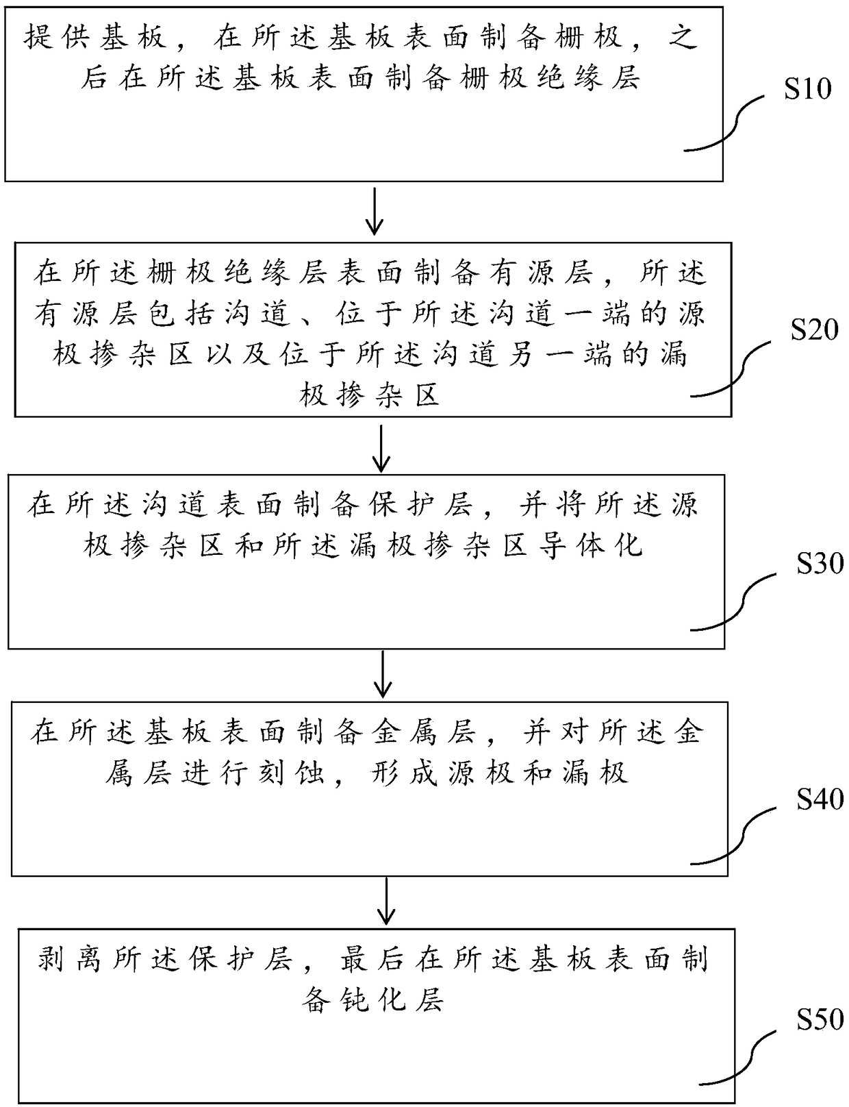
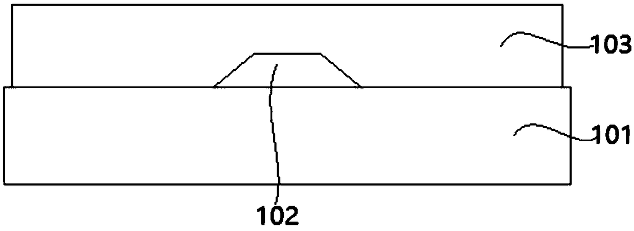
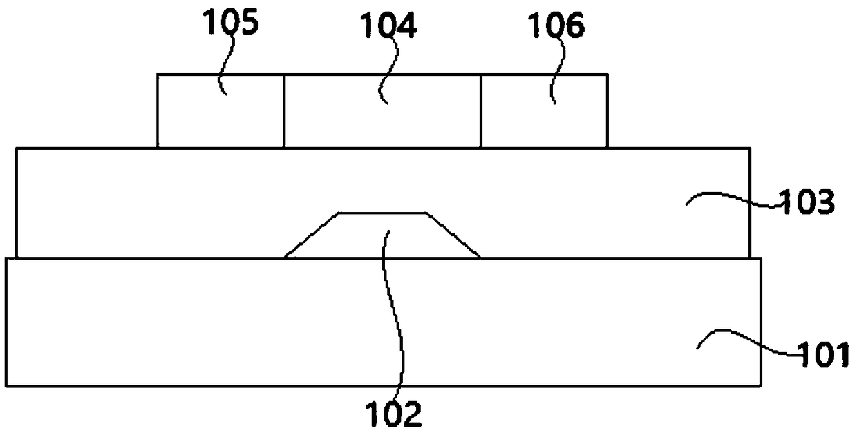
[0034] The following descriptions of the various embodiments refer to the accompanying drawings to illustrate specific embodiments in which the invention may be practiced. The directional terms mentioned in the present invention, such as [top], [bottom], [front], [back], [left], [right], [inside], [outside], [side], etc., are only for reference The orientation of the attached schema. Therefore, the directional terms used are used to illustrate and understand the present invention, but not to limit the present invention. In the figures, structurally similar elements are denoted by the same reference numerals.

[0035] The present invention is aimed at the existing TFT array substrate. Due to the poor adhesion between the source and drain electrodes and the substrate or gate insulating layer in the manufacturing process of the TFT array substrate, it diffuses to the channel of the active layer, thereby causing additional barrier layer materials to be added. This embodiment can...


PUM


Abstract

The invention provides a manufacturing method of a TFT array substrate. The method comprises: providing a substrate; sequentially preparing a gate electrode, a gate insulating layer and an active layer on the surface of the substrate, wherein, the active layer comprises a channel, a source doping region and a drain doping region; preparing a protective layer on the channel surface and conducting the source doped region and the drain doped region; forming a source electrode and a drain electrode on the surface of the substrate; stripping off the protective layer and finally preparing a passivation layer on the surface of the substrate. The invention also provides a TFT array substrate made by using the manufacturing method of the TFT array substrate, the method has the beneficial effects: the invention provides a manufacturing method of a TFT array substrate and the TFT array substrate, As the source dope region and the drain doping region are conductive, the adding of an extra barrierlayer material is avoided, the etching difficulty is further reduced, the channel loss of the active layer is further prevented, and the production cost of the TFT array substrate is finally reduced.

Description

technical field [0001] The invention relates to the field of flat panel display technology, in particular to a method for manufacturing a TFT array substrate and the TFT array substrate. Background technique [0002] At present, TFT-LCD (Thin Film Transistor-Liquid Crystal Display Panel) is widely used in portable electronic products such as mobile phones and PDAs due to its advantages such as micro power consumption, low operating voltage, no X-ray radiation, high definition, and small size. Among them, TFT is a switch to control light emission, which is the key to realize the large size of liquid crystal display, and is directly related to the development direction of high-performance flat panel display. At present, the bottom-gate IGZO (Indium Gallium Zinc Oxide, Indium Gallium Zinc Oxide) in the TFT structure is damaged in the etching process due to the selection ratio and other problems in the production process, causing IGZO surface defects, affecting device leakage cu...

Claims


Application Information

Patent Timeline
Patent Type & Authority Applications(China)
IPC IPC(8): H01L21/77H01L27/12
CPCH01L27/1214H01L27/1259H01L27/1225H01L27/1248H01L29/66969
Inventor 章仟益
Owner TCL CHINA STAR OPTOELECTRONICS TECH CO LTD
Why Eureka
Try Eureka