Run length-based one-scan connected component labeling method and hardware structure

A connected domain labeling and run-length technology, applied in the field of dedicated hardware accelerators for embedded image processing, can solve the problems of hardware resource overhead and power consumption, the performance is greatly affected by the system bandwidth, and the circuit processing speed is restricted.

Active Publication Date: 2018-11-23
NORTHWESTERN POLYTECHNICAL UNIV
View PDF7 Cites 1 Cited by
  • Summary
  • Abstract
  • Description
  • Claims
  • Application Information

AI Technical Summary

Problems solved by technology

[0004] Hardware connected domain marking can also be divided into three categories: single scan, double scan and multiple scans according to the number of scans of the input binary image: ① The hardware connected domain marking of single scan is mainly based on the boundary pursuit algorithm. For example, Hedberg designed a connected domain labeling hardware circuit for feature extraction (Implementation of a LabelingAlgorithm based on Contour Tracing with Feature Extraction). Although the hardware architecture can achieve a processing speed of 25 frames per second, the resolution of the input image is only 320× 240, and the demand for on-chip storage resources is greater than 1M bits
② Two scans to realize the hardware structure of the connected domain marking function. Generally, the first scan gives each foreground pixel a pre-mark value, and the second scan determines the final mark value of the foreground pixel according to the equivalence relationship of the mark value. For example, Yang based on the register array Implemented a VLSI architecture design for a fast parallel label assignment in binary image (VLSI architecture design for a fast parallel label assignment in binary image). When a high-resolution image is input and contains many connected regions, the architecture needs to consume a lot of hardware resources, and at the same time The processing speed of the circuit will be restricted
[0008] 3) Minimize the demand for on-chip storage resources. Connectivity markers generally need to temporarily store a large number of intermediate results in the on-chip storage module to avoid frequent access to external memory when used again, resulting in poor performance. However, excessive on-chip storage resource requirements will cause Hardware resource overhead and power consumption exceed design thresholds
[0009] At present, the connected domain marking method and its hardware implementation mainly involve two types of single scan and double scan: the single scan is based on the contour tracking method, the access to the external memory is irregular, and the demand for on-chip storage resources is large; the connected domain is scanned twice The main problem of the marking hardware structure is that for higher resolution images, the on-chip storage resource requirements are large, and because the image needs to be scanned twice, the performance is greatly affected by the system bandwidth

Method used


Image

  • Run length-based one-scan connected component labeling method and hardware structure
  • Run length-based one-scan connected component labeling method and hardware structure
  • Run length-based one-scan connected component labeling method and hardware structure

Examples


Embodiment Construction

[0044] Now in conjunction with embodiment, accompanying drawing, the present invention will be further described:

[0045] The purpose of the present invention is to provide a binary image connected domain marking method and hardware structure with less hardware resource consumption, which is realized by the following scheme:

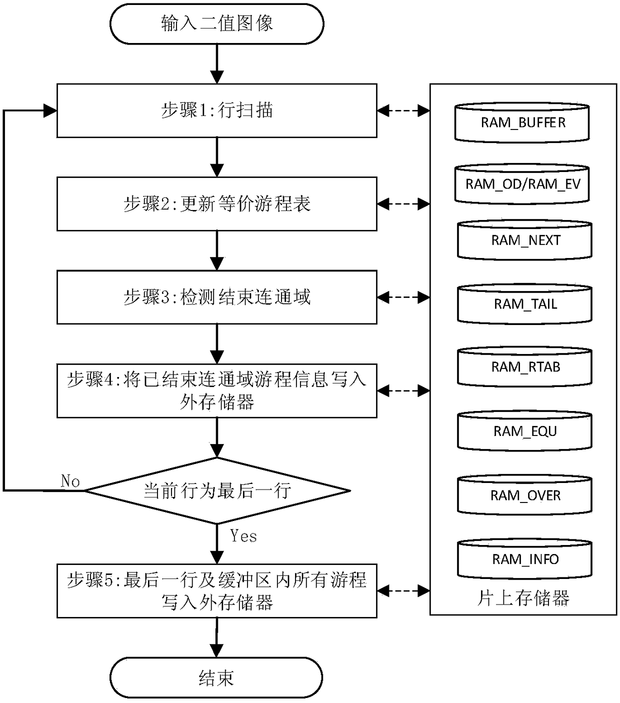
[0046] 1. A new type of connected domain labeling method, the process is as follows figure 1 As shown, it is divided into the following steps: ① Simultaneously scan two adjacent lines of the input binary image, and record the equivalent run between the two lines at the same time; ② Update the equivalent run table after scanning; ③ Detect that the connection has ended domain, and write the run of the connected domain that has ended into the external memory; ④ if the current line is the last line, write the line and all the runs in the run buffer to the external memory, otherwise, repeat all steps.

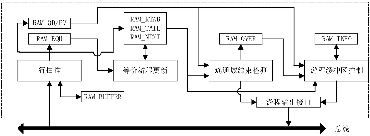
[0047] 2. Connected domain marking hardware accelerat...


PUM


Abstract

The invention relates to a run length-based one-scan connected component labeling method and hardware structure. The method comprises the steps of (1) simultaneously scanning two adjacent rows of an input binary image, and recording equivalent run length between the two rows; (2) updating an equivalent run length table after the scanning is completed; (3) detecting a completed connected component,and writing the run length of the completed connected domain into an external memory; and (4) if the current row is the last row, writing all the run lengths in the row and a run length buffer into the external memory, otherwise, repeatedly executing all the steps.

Description

technical field [0001] The invention belongs to the field of special hardware accelerators for embedded image processing, and mainly relates to a run-length-based single-scan binary image connected domain marking algorithm and hardware implementation structure. The invention can reduce the requirement of on-chip storage resources, and process higher-resolution binary images in real time, and is suitable for embedded image processing systems. Background technique [0002] Connected domain marking is mainly performed on binary images, where the pixel values ​​of binary images only consist of two values, "0" and "1", "1" represents foreground pixels, and "0" represents background pixels. In the binary image, the image subset S composed of foreground pixels, if any two pixels P and R have a path from P to R, then P and R are said to be connected in S, and the image subset The set S becomes a connected domain. According to the different platforms on which connected domain marki...

Claims


Application Information

Patent Timeline
Patent Type & Authority Applications(China)
IPC IPC(8): G06T1/20
CPCG06T1/20
Inventor 赵晨葛兴姚英朋苗兆伟高武
Owner NORTHWESTERN POLYTECHNICAL UNIV
Why Eureka
Try Eureka