Semiconductor integrated circuit device

A technology of integrated circuits and semiconductors, which is applied in the manufacture of semiconductor devices, circuits, semiconductor/solid-state devices, etc., can solve the problems of increasing the area of ​​semiconductor integrated circuits, and achieve the effect of ensuring power supply capability and ESD protection capability

Active Publication Date: 2018-11-23
SOCIONEXT INC
View PDF5 Cites 0 Cited by
  • Summary
  • Abstract
  • Description
  • Claims
  • Application Information

AI Technical Summary

Problems solved by technology

This can be solved by increasing the number of I / O cells used for power supply in each I / O cell column, but in this case there is a problem that the area of ​​the semiconductor integrated circuit is further increased

Method used


Image

  • Semiconductor integrated circuit device
  • Semiconductor integrated circuit device
  • Semiconductor integrated circuit device

Examples


no. 1 approach

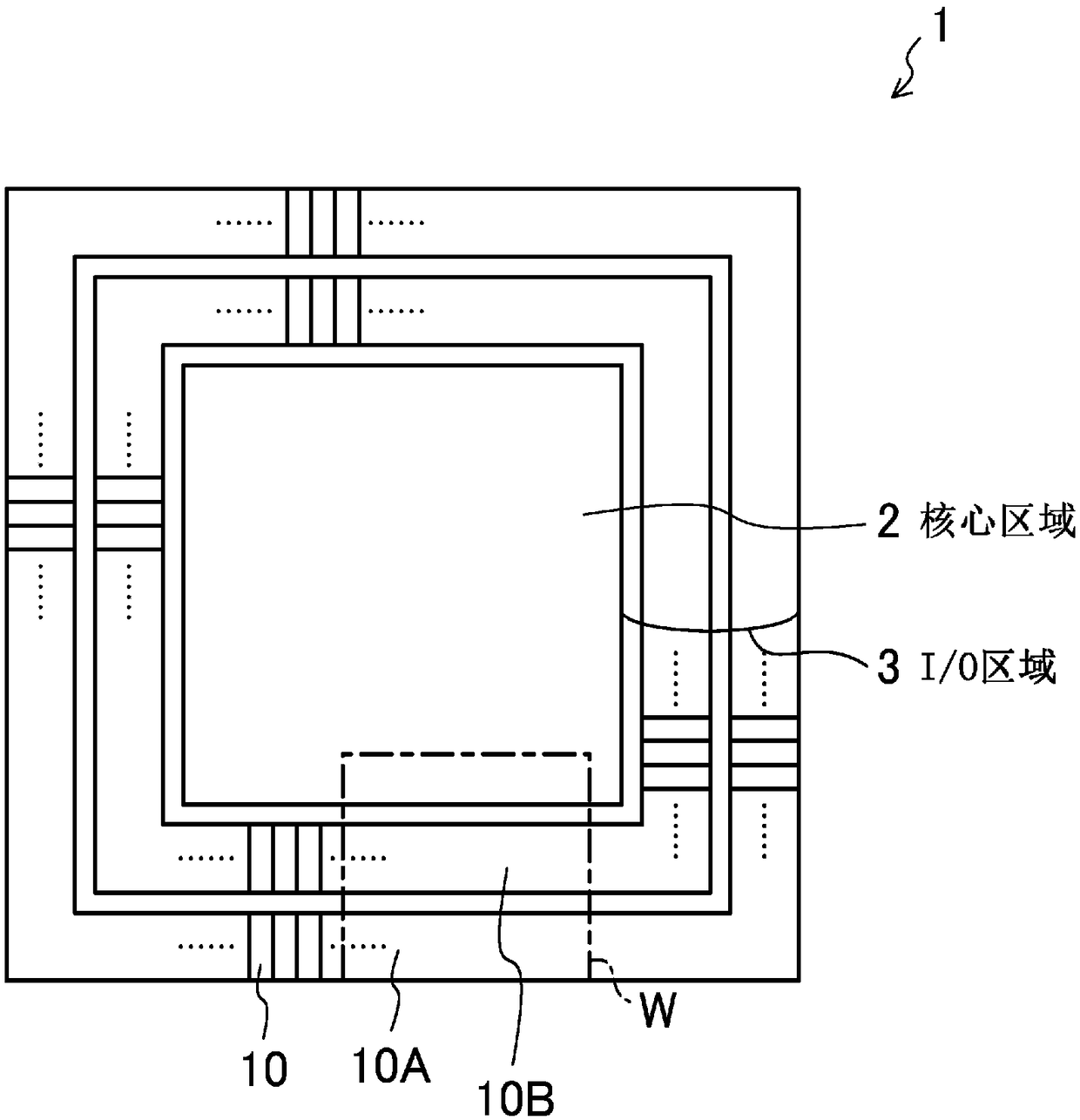
[0025] figure 1 It is a plan view schematically showing the overall structure of the semiconductor integrated circuit device according to the embodiment. figure 1 The illustrated semiconductor integrated circuit device 1 includes a core area 2 in which an internal core circuit is formed and an I / O area 3 provided around the core area 2 and formed with an interface circuit (I / O area 3). O circuit). Two I / O cell columns 10A, 10B are provided annularly in the I / O region 3 and around the peripheral portion of the semiconductor integrated circuit device 1 . Although in figure 1 Although the illustration is simplified in FIG. 1 , a plurality of I / O cells 10 constituting an interface circuit are arranged in the I / O cell columns 10A and 10B, respectively. exist figure 1 Although illustration is omitted in , a plurality of external connection pads are arranged in the semiconductor integrated circuit device 1 .

[0026] figure 2 is a plan view showing a configuration example of t...

no. 2 approach

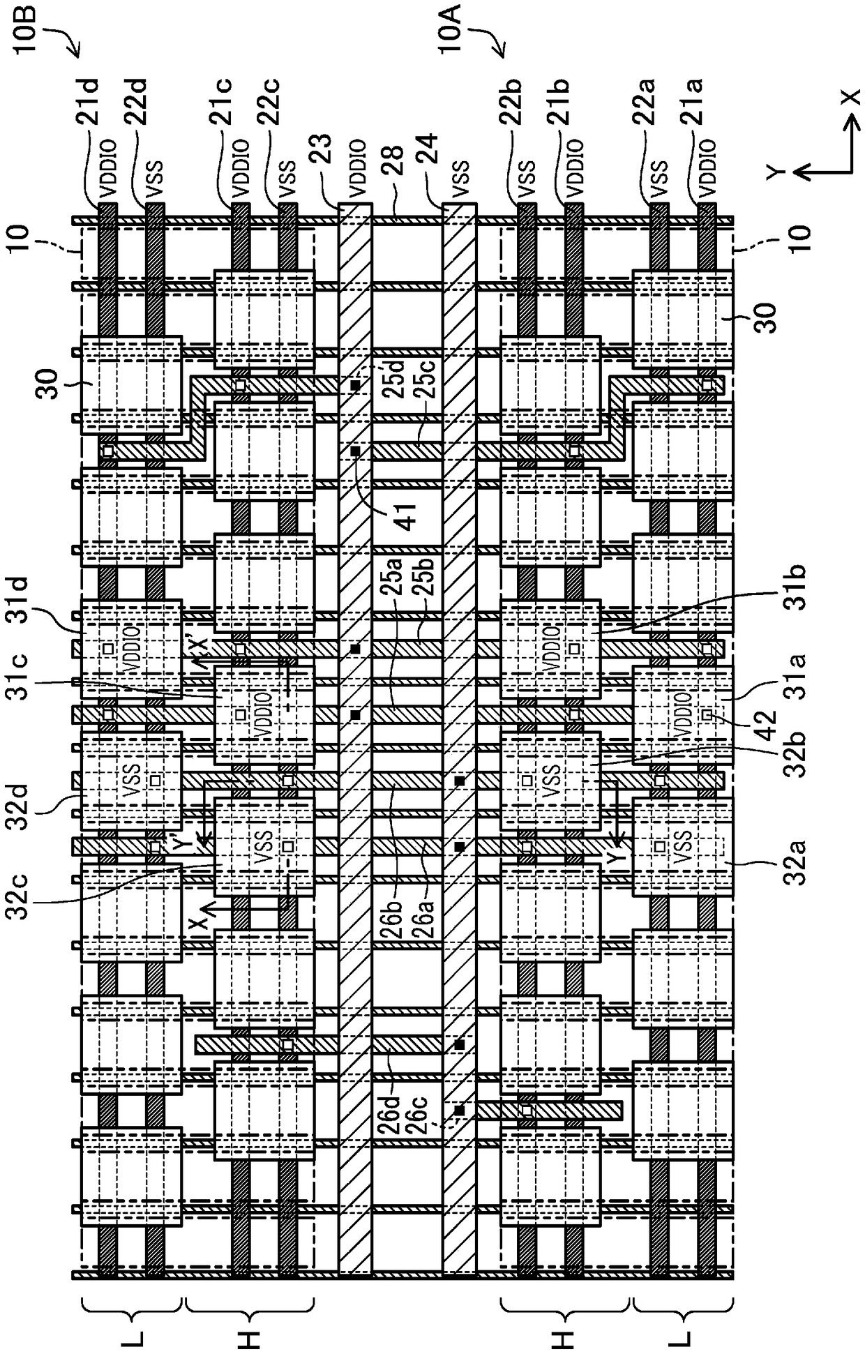
[0061] Figure 6 is a diagram showing a configuration example of the I / O region 3 of the semiconductor integrated circuit device according to the second embodiment, and corresponds to figure 1 Enlarged view of part W in . exist Figure 6 In the example of the configuration, three kinds of power supply potentials VDD, VDDIO18, and VDDIO33 are supplied. For example, the power supply potential VDD is 0.9V, the power supply potential VDDIO18 is 1.8V, and the power supply potential VDD33 is 3.3V. It should be noted that, in Figure 6 In , illustration of the internal structure of the I / O unit, signal wiring, etc. is omitted.

[0062] exist Figure 6 Among them, the two columns of I / O cell columns 10A, 10B respectively have Figure 6A plurality of I / O cells 10 (the cell area is indicated by a two-dot chain line) arranged in the lateral direction, that is, the direction extending along the side of the semiconductor integrated circuit device 1), wherein the X direction correspon...


PUM


Abstract

The objective of the invention is to provide a configuration in a semiconductor integrated circuit device whereby ESD protection capabilities and capabilities to supply a power source to I / O cells canbe sufficiently maintained without leading to an increase in the circuit surface area. In this invention, intra-column power source wirings (21a to 21d) provided in I / O cell columns (10A, 10B) are connected via power source wirings (25a to 25d) to a power source wiring (23) provided between the I / O cell columns (10A, 10B). The power source wiring (23) is greater in thickness than each of the intra-column power source wirings (21a to 21d).

Description

technical field [0001] The present disclosure relates to a semiconductor integrated circuit device formed with a core region and an I / O region. Background technique [0002] In recent years, the scale of semiconductor integrated circuits has continued to expand, and the number of input and output signals has also increased. Therefore, there is a problem that if the input / output cells (I / O cells) are arranged in a single array around the core area, the area of ​​the semiconductor integrated circuit is determined by the I / O cells, and sometimes a device with a semiconductor integrated circuit is formed. The area of ​​the integrated semiconductor integrated circuit device will increase. [0003] In Patent Document 1, there is disclosed a structure of a semiconductor integrated circuit in which I / O cells are arranged in multiples on a peripheral portion of a circuit. With this structure, it is avoided that the area of ​​the semiconductor integrated circuit is determined by the...

Claims


Application Information

Patent Timeline
IPC IPC(8): H01L21/822H01L21/3205H01L21/768H01L21/82H01L23/522H01L27/04
CPCH01L27/0292H01L23/5286H01L23/50H01L27/0248
Inventor 广濑雅庸中村敏宏
Owner SOCIONEXT INC
Why Eureka
Try Eureka