Card and Manufacturing Method

a manufacturing method and card technology, applied in the field of card energy transmission, can solve the problems of relatively complicated card manufacturing and the need for windings of antennas to be embedded in the substrate layer, and achieve the effect of simple electrical contact and easy electrical conta

Inactive Publication Date: 2007-08-02
ASSA ABLOY AB
View PDF5 Cites 22 Cited by
  • Summary
  • Abstract
  • Description
  • Claims
  • Application Information

AI Technical Summary

Benefits of technology

[0013] The coil connections for the substrate layer are easily electrically and mechanically connected to the connections for the chip module by means of pressure contact as the result of lamination. This ensures a particularly simple electrical contacting.

Problems solved by technology

A disadvantage herein is that the windings of the antenna must be embedded in the substrate layer.
Manufacture of the card is relatively complicated due to the need for pressing the eyes of the chip module into the substrate layer.

Method used


Image

  • Card and Manufacturing Method
  • Card and Manufacturing Method

Examples


Embodiment Construction

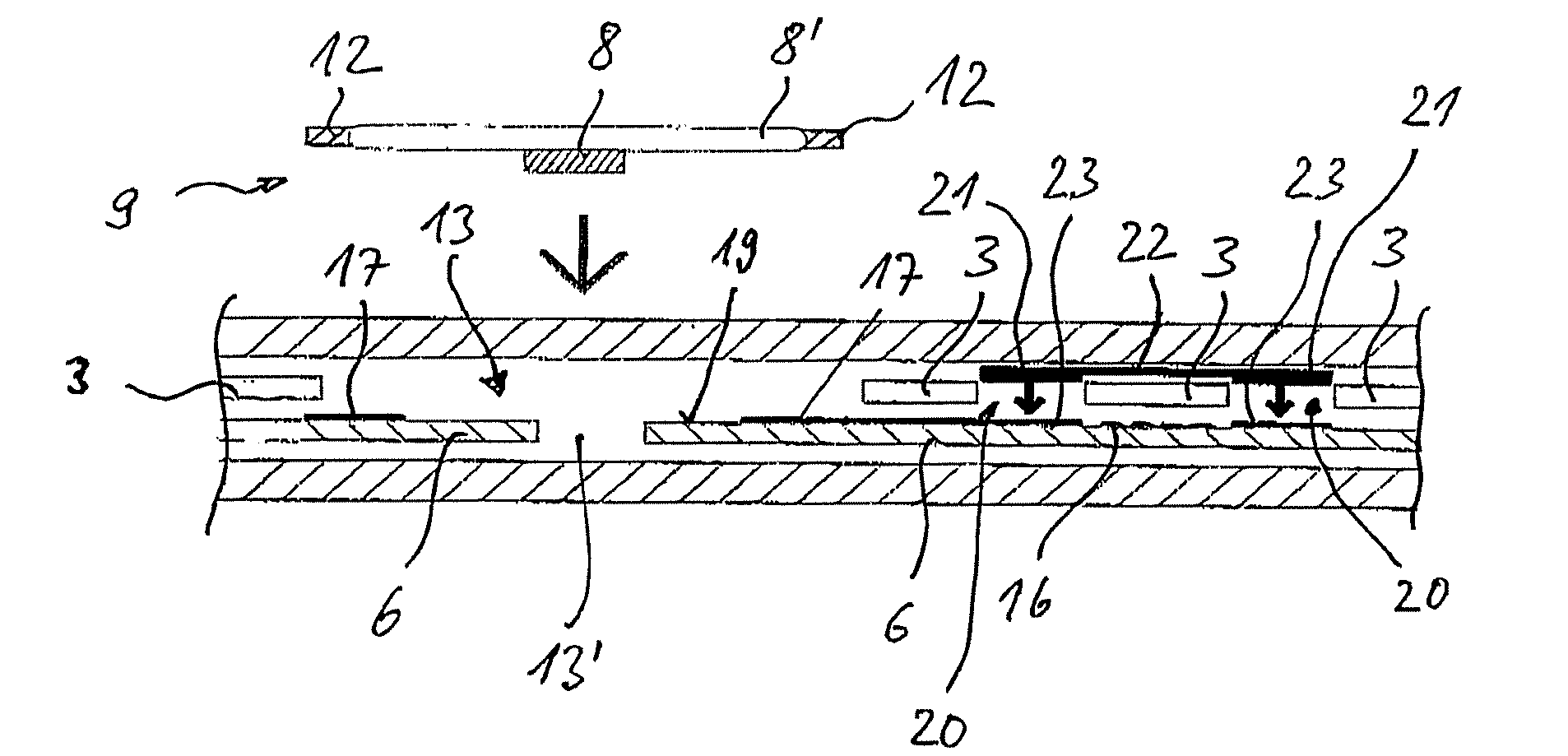
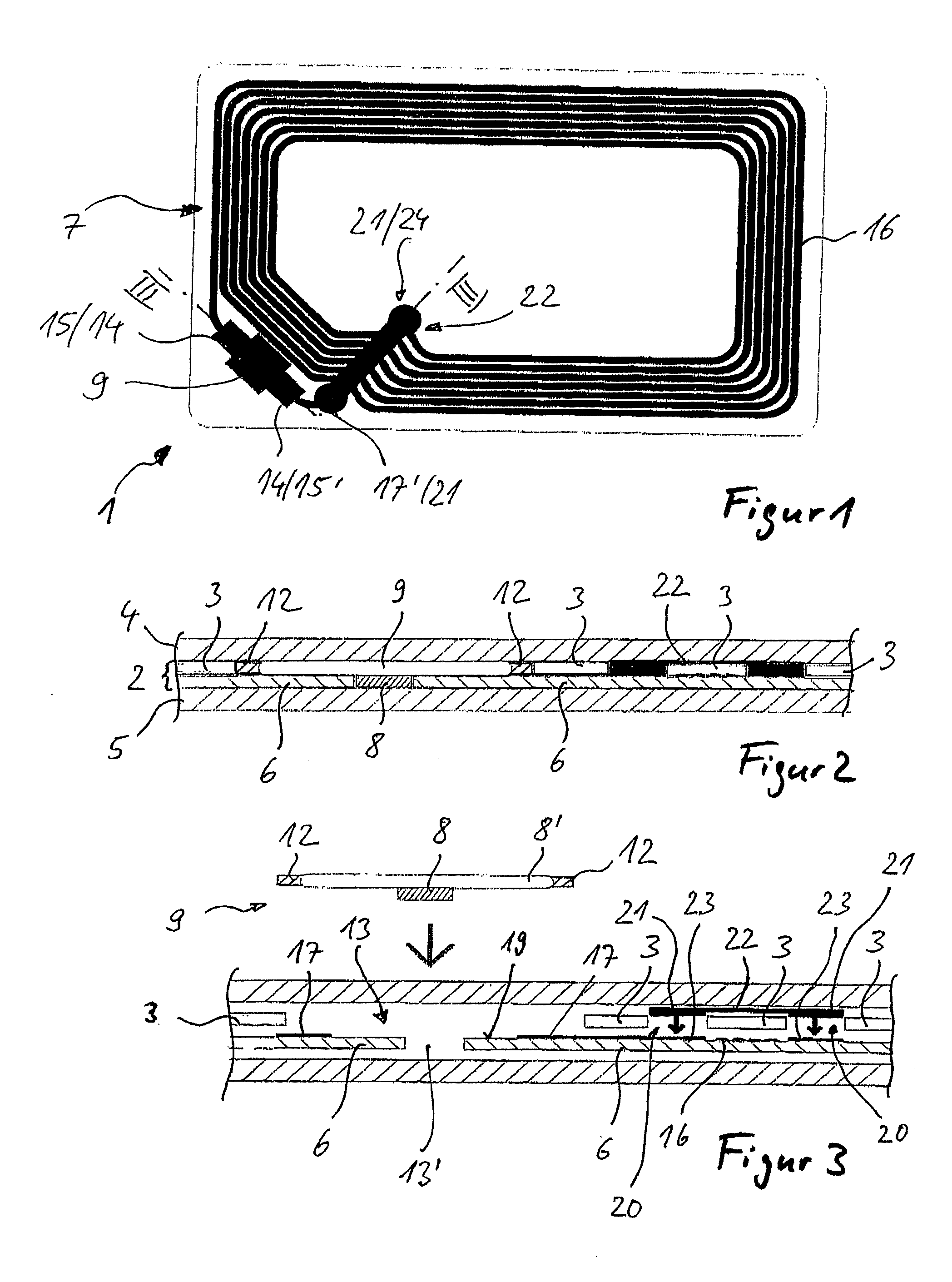
[0019] A card according to the invention for contactless data and / or energy transmission by means of external devices has a multilayer card body which is essentially composed of a prelaminate 1 as a semi-finished product and at least one printed layer (PVC layer), adjoining the prelaminate 1, with or without an additional transparent or thermally writable overlay layer.

[0020]FIGS. 1 through 3 illustrate a prelaminate 1 which is essentially composed of a core layer 2, an upper cover layer 4, and a lower cover layer 5.

[0021] The core layer 2 is composed of a substrate layer 6 to which an antenna coil 7 is applied. The antenna coil 7 preferably is applied by screen printing on the substrate layer 6.

[0022] The core layer 2 also has a chip module 9 and a compensation layer 3 which extend essentially in a common plane in contact with a top side 19 of the substrate layer 6. The chip module 9 has a chip 8 and a chip carrier 8′. The chip 8 is preferably situated in a middle region of the ...


PUM


Abstract

The invention relates to a card for contactless data and/or energy transmission by means of external devices, containing a multilayer card body which has a substrate layer for accommodating an antenna coil having exposed coil connections on a top side of the substrate layer which are connected in an electrically conductive manner to connections for a chip module containing a chip, the chip being enclosed in a recess in the substrate layer; the windings of the antenna coil extend on the top side of the substrate layer, and a compensation layer extends on the top side of the substrate layer; the compensation layer has a chip module opening for placing the chip module on the substrate layer, and has a bridge opening for the contacting of connections of an antenna bridge which extends transverse to the windings.

Description

FIELD OF THE INVENTION [0001] The invention relates to a card energy transmission by means of external devices, containing a multilayer card body which has a substrate layer for accommodating an antenna coil having exposed coil connections on a top side of the substrate layer which are connected in an electrically conductive manner to connections for a chip module containing a chip, the chip being enclosed in a recess in the substrate layer. [0002] The invention further relates to a method for manufacturing a card for contactless data and / or energy transmission by means of external devices, a chip module which bears a chip being connected to a substrate layer which has an antenna coil, and connections for the chip module being connected in an electrically conductive manner to coil connections for the antenna coil. BACKGROUND OF THE INVENTION [0003] For manufacturing a card for contactless data and / or energy transmission by means of external devices, it is known from DE 100 32 676 A1...

Claims


Application Information

Patent Timeline
Patent Type & Authority Applications(United States)
IPC IPC(8): H01L23/02H01L21/00
CPCG06K19/07749
Inventor WOLNY, ROBERT
Owner ASSA ABLOY AB
Why Eureka
Try Eureka