Monitoring method for electromagnetic immunity of CMOS inverter

An electromagnetic immunity, inverter technology, applied in the direction of single semiconductor device testing, instrumentation, measuring electricity, etc., can solve the problem of not intuitively monitoring the abnormal operation of the inverter, etc.

Inactive Publication Date: 2018-11-30
SOUTH CHINA UNIV OF TECH
View PDF5 Cites 4 Cited by
  • Summary
  • Abstract
  • Description
  • Claims
  • Application Information

AI Technical Summary

Problems solved by technology

[0004] The purpose of the present invention is to provide a method for monitoring the electromagnetic immunity of CMOS inverters in order to solve the problem that there is no method for intuitively monitoring the abnormal operation of the inverter after being electromagnetically disturbed in the prior art

Method used


Image

  • Monitoring method for electromagnetic immunity of CMOS inverter
  • Monitoring method for electromagnetic immunity of CMOS inverter

Examples


Embodiment 1

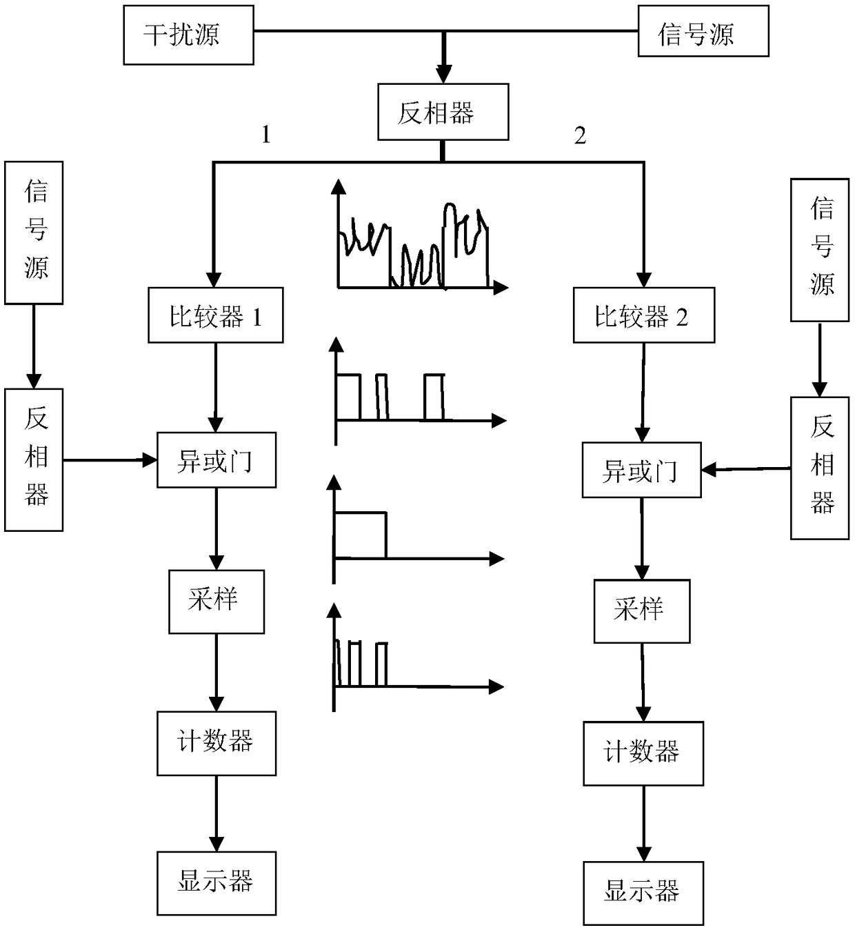
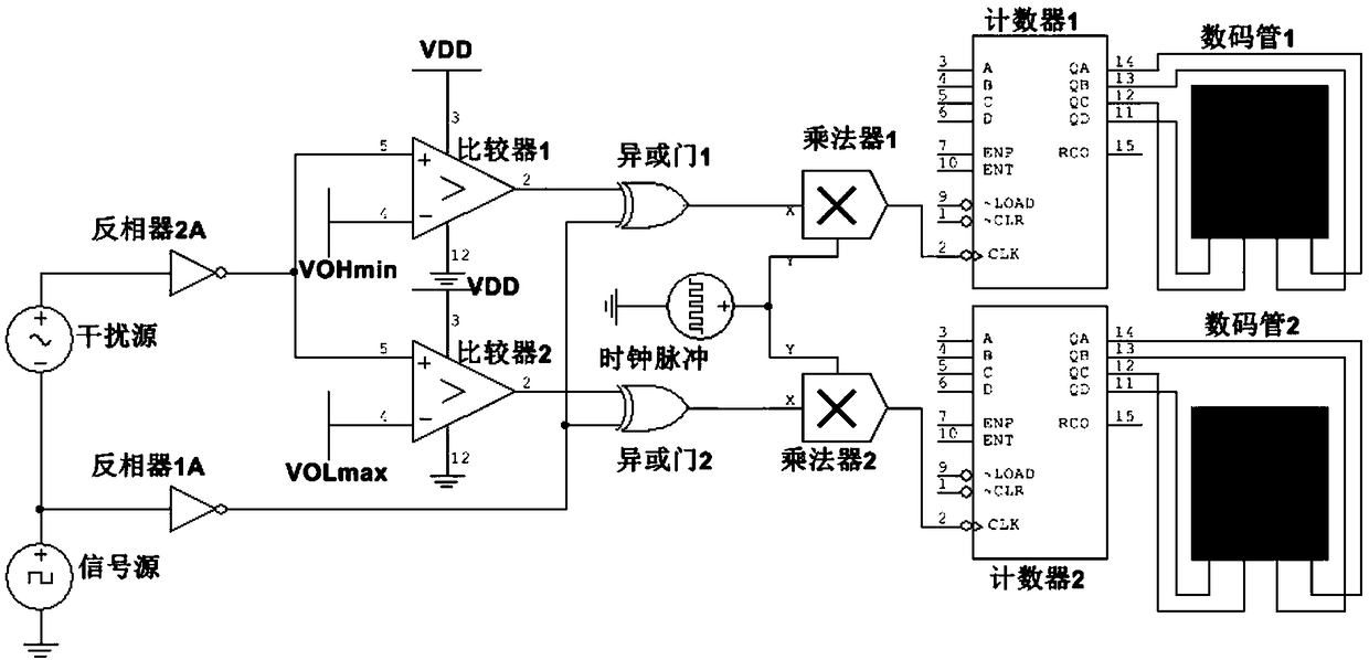
[0019] Such as figure 1 As shown, a method for monitoring the electromagnetic immunity of a CMOS inverter, the specific workflow is as follows: the output signal of the signal source is an interactive high and low level, and the signal is divided into two channels for processing, one is input to the inverter 1, and the output The first inverting signal is input to the inverter 2 after the interference source interferes with the original signal in the other channel, and the second inverting signal is output. This method can separately discuss the situation that the input is high level and low level, and the two-way processing methods can respectively detect the abnormal operation states of the input high level and low level. The voltage comparator 1 and the voltage comparator 2 are single-limit comparators, and the comparison levels are VOHmin and VOLmax respectively, and are used to convert the analog signal into a digital signal. The signal output by the inverter after being...


PUM


Abstract

The invention discloses a monitoring method for the electromagnetic immunity of a CMOS inverter. A monitoring circuit adopted is mainly composed of the inverter, a comparator, an exclusive-OR gate, amultiplier, a counter, a display and the like. The monitoring method refers to a method for error code detection of a communication system, a more intuitive statistical monitoring way is adopted, an output signal of the inverter with electromagnetic interference and an output signal of the inverter without the electromagnetic interference are taken as two input ends of the exclusive-OR gate, if the level values of the two signals are different, the output of the exclusive-OR gate is high level, and the number of high levels output by the exclusive-OR gate is recorded and displayed. The monitoring method can obtain the abnormal operation of the inverter and the degree of abnormal operation in real time and quantitatively under certain electromagnetic interference.

Description

technical field [0001] The invention relates to the technical field of electromagnetic interference, in particular to a method for monitoring the electromagnetic immunity of a CMOS inverter. Background technique [0002] There are many monitoring methods for abnormal operation of integrated circuits, such as output signal voltage limit and delay limit, current consumption of the circuit under test, spectral shape of output current or propagation delay, etc. It is very complicated to monitor several criteria in the same experiment. For an inverter, the most important criterion is the voltage level as a function of time. Due to the development of the manufacturing process, the density of transistors per square millimeter is gradually increased, and the I / O voltage and nuclear voltage are gradually reduced. This means that under the same electromagnetic environment, the chip with a smaller process size has a lower noise tolerance. It will be more susceptible to harassment, tha...

Claims


Application Information

Patent Timeline
Patent Type & Authority Applications(China)
IPC IPC(8): G01R31/26
CPCG01R31/2603
Inventor 张亚芳贾亚俊黎天赐陈武喝
Owner SOUTH CHINA UNIV OF TECH
Why Eureka
Try Eureka