A detection method and detection device for a display panel

A technology of a display panel and a detection method, which is applied to static indicators, instruments, etc., can solve problems such as inconvenient maintenance, inability to charge and discharge pixel electrodes well, and allowable range of threshold voltage errors of thin film transistors.

Active Publication Date: 2021-05-11
NANJING BOE DISPLAY TECH CO LTD
View PDF6 Cites 0 Cited by
  • Summary
  • Abstract
  • Description
  • Claims
  • Application Information

AI Technical Summary

Problems solved by technology

Due to process errors, such as figure 1 As shown, due to reasons such as foreign matter in the film layer, the transfer characteristic curve (Vg-Id curve) of one or more thin film transistors may shift to the right, resulting in the threshold voltage Vth of the abnormal thin film transistor being greater than the allowable range of error
However, this type of defect is difficult to be effectively detected during post-break inspection, and is usually found in module inspection, reliability confirmation, or in the hands of customers
[0004] In the module detection, the scanning signal is scanned line by line, the gate turn-on voltage Vgh and the gate threshold voltage Vgl are switched, the abnormal thin film transistor cannot charge and discharge the pixel electrode well, and it is easy to show defects such as bright spots or rough pictures, thus Detect TFT right shift defect
However, it is difficult to locate the coordinates of the abnormal thin film transistors detected in the module inspection stage, which is not convenient for maintenance and there is a risk of failure in the repair
Therefore, it is impossible to effectively detect the right-shift defect of TFT characteristics after breaking, which causes waste of materials and manpower, and also increases quality risks.

Method used


Image

  • A detection method and detection device for a display panel
  • A detection method and detection device for a display panel
  • A detection method and detection device for a display panel

Examples


Embodiment Construction

[0033] In order to more clearly illustrate the embodiments of the present invention or the technical solutions in the prior art, the specific implementation manners of the present invention will be described below with reference to the accompanying drawings. Obviously, the accompanying drawings in the following description are only some embodiments of the present invention, and those skilled in the art can obtain other accompanying drawings based on these drawings and obtain other implementations.

[0034] In order to make the drawing concise, each drawing only schematically shows the parts related to the present invention, and they do not represent the actual structure of the product. In addition, to make the drawings concise and easy to understand, in some drawings, only one of the components having the same structure or function is schematically shown, or only one of them is marked.

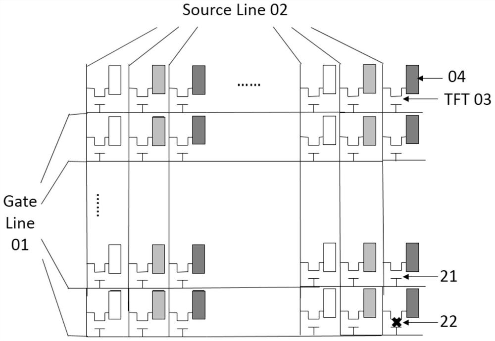
[0035] figure 2 It is a display panel structure, including criss-crossing gate lines 01...


PUM


Abstract

The invention discloses a detection method of a display panel. The detection method controls the voltage of the source line to decrease from a high source voltage to a low source voltage when the gate line is at the gate detection voltage, so that the normal thin film transistor corresponding The pixel is changed from a bright picture to a dark picture, so that the pixel corresponding to the abnormal thin film transistor with TFT characteristic right-shift defect remains a bright picture, so that the pixel corresponding to the abnormal thin film transistor is highlighted in the form of a bright spot in the overall black picture, accurate and effective detection Pixels with TFT characteristic right-shift defects are obtained; the invention also discloses a detection device for a display panel.

Description

technical field [0001] The invention relates to the field of display technology, in particular to a detection method of a display panel and a detection device thereof. Background technique [0002] In the existing manufacturing process, the display panel is tested in multiple steps, including cutting the mother board into multiple display panels (panels), and then performing lighting detection by inputting various detection signals to the display panel; it also includes completing the chip ( After the IC) is crimped, the display module is again tested for lighting to detect defects in the crimping process or missed defects caused by the post-break inspection. [0003] In the post-breaking detection (SL lighting) stage, low-frequency drive is used, so it can only be detected normally when the semiconductor conductive channel of the thin film transistor (TFT) is completely disconnected or the threshold voltage of the thin film transistor is much higher than the gate turn-on vo...

Claims


Application Information

Patent Timeline
Patent Type & Authority Patents(China)
IPC IPC(8): G09G3/00
CPCG09G3/006
Inventor 王再武杭传静蔡扬沙先龙
Owner NANJING BOE DISPLAY TECH CO LTD
Why Eureka
Try Eureka