An array substrate, a display device, and a mask plate

An array substrate and mask technology, which is applied to semiconductor/solid-state device parts, semiconductor devices, electrical components, etc., can solve the problems of burns and overheating of the lead insulation layer of the first power line

Active Publication Date: 2020-06-26
BOE TECH GRP CO LTD +1
View PDF5 Cites 0 Cited by
  • Summary
  • Abstract
  • Description
  • Claims
  • Application Information

AI Technical Summary

Problems solved by technology

[0005] Embodiments of the present invention provide an array substrate, a display device, and a mask plate, which are used to solve the problem of burning the insulating layer above the lead of the first power lead due to local overheating on the lead of the first power lead

Method used


Image

  • An array substrate, a display device, and a mask plate
  • An array substrate, a display device, and a mask plate
  • An array substrate, a display device, and a mask plate

Examples


Embodiment Construction

[0030] The following will clearly and completely describe the technical solutions in the embodiments of the present invention with reference to the accompanying drawings in the embodiments of the present invention. Obviously, the described embodiments are only some, not all, embodiments of the present invention. Based on the embodiments of the present invention, all other embodiments obtained by persons of ordinary skill in the art without making creative efforts belong to the protection scope of the present invention.

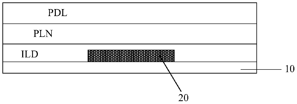
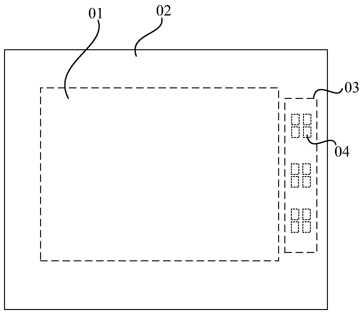
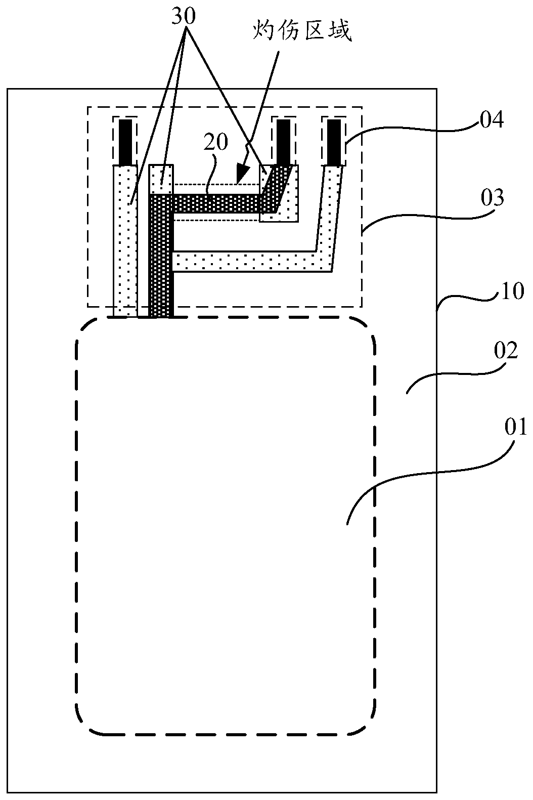
[0031] Such as figure 2 As shown, the array substrate is divided into a display area 01 and a non-display area 02 , the non-display area 02 includes a binding area 03 , and the binding area 03 includes a Pad area 04 . The area in the non-display area 02 for binding an IC (Integrated Circuit, integrated circuit) is called a binding area 03 , and the area in the binding area 03 where the IC is connected to the wiring on the array substrate is called a Pad area ...


PUM


Abstract

The invention provides an array substrate, a display device and a mask plate, relates to the display technical field, and solves the problems that an insulation layer above a first power line lead isburned due to the local overheating condition on the first power line lead. The array substrate comprises a binding zone that has the first power line lead and a signal line lead; the signal line leadis arranged on one side, far away from the substrate, of the first power line lead; the binding zone also has a heat conductive pattern arranged on one side, far away from the substrate, of the firstpower line lead; the positive projection of the signal line lead on the substrate covers a portion of the positive projection of the first power line lead on the substrate; the positive projection ofthe heat conductive pattern on the substrate overlaps with the other portion of the positive projection of the first power line lead on the substrate.

Description

technical field [0001] The present invention relates to the field of display technology, in particular to an array substrate, a display device, and a mask plate. Background technique [0002] OLED (Organic Light-Emitting Diode, organic electroluminescent diode) display device has thin, light, wide viewing angle, active light emission, continuously adjustable light color, low cost, high color gamut, high contrast, fast response speed, and low energy consumption. The advantages of small size, low driving voltage, wide operating temperature range, simple production process, high luminous efficiency and flexible display have been listed as the next generation display technology with development prospects. [0003] In the prior art, the preliminarily prepared display panel has the following problems: on the one hand, there are many quantum dots in the display panel due to the presence of free electrons inside the display panel; Stablize. Based on this, before the display panel ...

Claims


Application Information

Patent Timeline
Patent Type & Authority Patents(China)
IPC IPC(8): H01L23/367H01L27/12
CPCH01L23/367H01L27/124
Inventor 薛智勇彭利满白妮妮刘亮亮刘祺
Owner BOE TECH GRP CO LTD
Why Eureka
Try Eureka