
A Fast Fault Tolerance Method for Normally Open Defects in Nano CMOS Circuits

A defect and nano-technology, applied in the field of fault-tolerant mapping of nano-CMOS circuits, can solve problems such as low mapping success rate, slow mapping method speed, and poor solution quality, and achieve the effects of reducing the mapping area, simplifying the difficulty, and eliminating the impact

Active Publication Date: 2021-10-29
NINGBO UNIV
View PDF8 Cites 0 Cited by
  • Summary
  • Abstract
  • Description
  • Claims
  • Application Information

AI Technical Summary

Problems solved by technology

[0009] The technical problem to be solved by the present invention is to provide a nano-CMOS circuit under the constraints of connected domains and defects of the nano-CMOS circuit in view of the existing mapping methods such as slow speed, poor solution quality, and low mapping success rate. A Fast Fault Tolerant Method for Normally Open Defects

Method used


Image

  • A Fast Fault Tolerance Method for Normally Open Defects in Nano CMOS Circuits
  • A Fast Fault Tolerance Method for Normally Open Defects in Nano CMOS Circuits
  • A Fast Fault Tolerance Method for Normally Open Defects in Nano CMOS Circuits

Examples


Embodiment 1

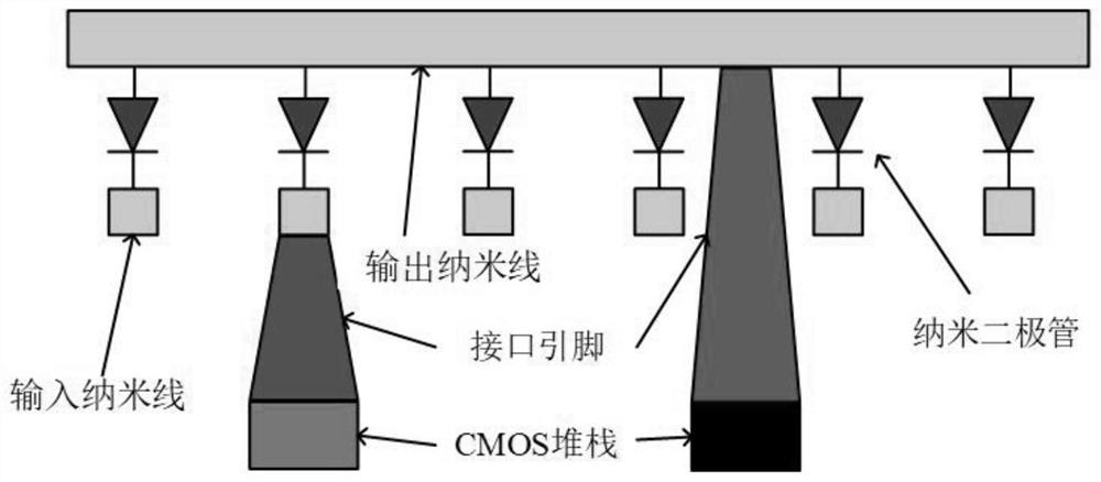
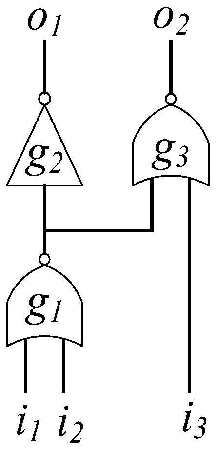
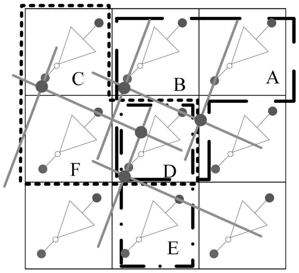
[0042] Embodiment 1: Take the simple circuit of three inputs and two outputs shown in Fig. 2 (a) as an example to carry out layering, and its fault-tolerant mapping layered schematic diagram on the defective nanometer CMOS circuit is shown in Figure 4 , 3 input terminals and 3 nodes are respectively mapped on the unit A-E unit, in which the nanodiode 1 between unit BD has a normally-on defect, the output nanowire of unit C is broken at 2, and the bottom CMOS unit of unit E is at 3 There is an unavailable normally open defect. Figure 4 The fast fault-tolerant method for the shown nanometer CMOS circuit includes the following steps:

[0043] Step ①: According to formula (1), calculate the total number of effective defects in the nano-CMOS circuit n def =5; Calculate y (0)=2, y (1)=2, y (2)=1 according to the defect distribution function of formula (2); From the boundary first unit of nanometer CMOS circuit, check unit C, successively B. The CMOS stack defects of A. After ins...

Embodiment 2

[0051] Embodiment 2: with Figure 5 The nano-CMOS circuit structure with a size of 5×4 is shown as an example, and the schematic diagram of the normally-on defect of the nano-diode is shown in Figure 5 .

[0052] Figure 5 The nano-CMOS circuit structure shown includes 20 nano-CMOS units, and the input nanowire of unit F can receive the output signals of unit A and unit B through programmable nano-diodes, and the The logic function; the input nanowire of unit F' can receive the output signal of unit C and unit D, and complete the logic function From Figure 5 It can be seen that the programmable nanodiode located at the intersection of the output nanowire of B and the input nanowire of F is normally on ( Figure 5 Indicated by the square 1 in the center), the programmable nanodiode located at the intersection of the output nanowire of D and the input nanowire of F' is normally on ( Figure 5 Indicated by square 2 in the middle), the actual logical function that can be ...

Embodiment 3

[0058] Embodiment 3: with Figure 6 The nano-CMOS circuit structure of 8×8 size is shown as an example, and the schematic diagram of its nano-diode normally-on defect is shown in Figure 6 .

[0059] When the output nanowire of unit A breaks at point a, the nanodiodes connected to the nanowire at point a and the nanometer CMOS circuit units connected to these nanodiodes cannot receive the output signal of unit A. For unit A, the range of the output connected domain of A is narrowed, and the basic function of the nano-CMOS circuit unit connected below point a remains unchanged, but the total number of units in the input connected domain is reduced by one unit A. Therefore, as long as the associated nodes avoid mapping nano-CMOS cells with broken nanowires and connected nano-CMOS cells beyond the broken point, the defective cells can continue to be used.

[0060] Figure 6 The fast fault-tolerant method for the normally-on defect of the shown nanometer CMOS circuit comprises ...


PUM


Abstract

The fast fault-tolerant method for the normally open defect of the nano-CMOS circuit disclosed by the present invention uses the connected domain modification of the nano-CMOS unit to remove the units with usable normally-open defects from their respective connected domains, and continue to connect with other units The defective unit is used rather than discarded, and the defective unit is properly utilized to improve the utilization rate of the unit and reduce the mapping area. At the same time, the nanometer CMOS circuit is divided into several smaller-scale arrays for local fault tolerance, which simplifies the difficulty of fault tolerance. Based on the local optimization results, the proposed method is verified by using the tabu search algorithm combined with the avoidance criterion, so as to improve the speed of eliminating normally open defects and the quality of fault-tolerant mapping, and accelerate the practical process of nano-CMOS circuit structure. The present invention can quickly eliminate the influence of the normally-on defect on the logic function of the nanometer CMOS circuit under the condition of improving the unit utilization rate and the mapping success rate, thereby effectively solving the fault-tolerant mapping problem of the nanometer CMOS circuit defect.

Description

technical field [0001] The invention relates to a nanometer CMOS circuit fault-tolerant mapping method, in particular to a fast fault-tolerant method for normally open defects of the nanometer CMOS circuit applied in the field of integrated circuits. Background technique [0002] With the continuous shrinking of the line width of the manufacturing process, traditional silicon-based CMOS integrated circuits are rapidly approaching the physical limit of the device, and the increase in manufacturing costs and microscopic quantum effects make it difficult for traditional technologies to meet the needs of current development. With the rapid development of nanoelectronics in recent years, people hope that emerging nanoelectronic devices and corresponding nanocircuits will continue the development of integrated circuits, so that circuits have higher integration density and operating frequency. [0003] In 2005, Likharev and his colleagues proposed the CMOS / nanowire / molecular hybrid...

Claims


Application Information

Patent Timeline
Patent Type & Authority Patents(China)
IPC IPC(8): H03K19/20H03K19/0948G11C29/12
CPCG11C29/12G11C2029/1208H03K19/0948H03K19/20
Inventor 夏银水查晓婧储著飞
Owner NINGBO UNIV
Learn More