Quick mapping method for normally open defect of nano CMOS circuit represented by matrix

A technology of matrix representation and mapping method, which is applied in the direction of electrical digital data processing, special data processing applications, instruments, etc., and can solve problems such as reducing the mapping area

Active Publication Date: 2020-04-24
NINGBO UNIV
View PDF4 Cites 0 Cited by
  • Summary
  • Abstract
  • Description
  • Claims
  • Application Information

AI Technical Summary

Problems solved by technology

[0009] The technical problem to be solved by the present invention is to provide a fast mapping method for normally-on defects of nano-CMOS circuits represented by a matrix under the constraints of connected domains of nano-CMOS circuits and the presence of normally-on defects for the deficiencies of the prior art. The method can simplify the complexity of circuit mapping, improve the efficiency and scale of circuit solving, reduce the mapping area, and quickly eliminate the influence of normally open defects on the logic function of nano-CMOS circuits while improving the utilization rate of cells and the success rate of mapping, so as to effectively solve the problem of Fault Tolerance Mapping of Normally Open Defects in Nano CMOS Circuits

Method used


Image

  • Quick mapping method for normally open defect of nano CMOS circuit represented by matrix
  • Quick mapping method for normally open defect of nano CMOS circuit represented by matrix
  • Quick mapping method for normally open defect of nano CMOS circuit represented by matrix

Examples


Embodiment Construction

[0051] The present invention will be further described in detail below in conjunction with the accompanying drawings and embodiments.

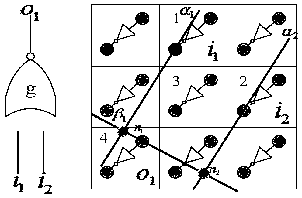
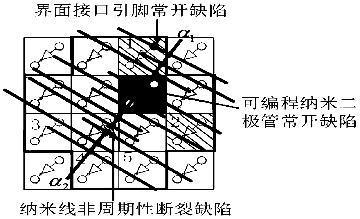
[0052] by Figure 4 (a) shows a NOR gate logic circuit containing 11 nodes as an example, and it is mapped to a 4×4 size in the form of a matrix Figure 5 The defective nano-CMOS circuit shown in (a) adopts the method of the present invention to carry out fast fault-tolerant mapping, specifically comprises the following steps:

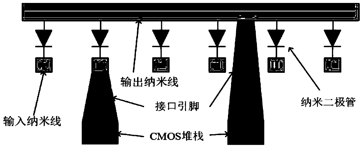
[0053] Step ①: For any nano-CMOS circuit including output nanowire layer, input nanowire layer, several programmable nano-diodes and bottom CMOS inverter array, if any programmable nano-diode is always in the off state, causing its The signal path between the connected two nanometer CMOS units is always disconnected, and the defect is defined as a programmable nanodiode normally-on defect; if any output nanowire or input nanowire breaks irregularly at the non-periodic breakpoint , causing the connected domain of the ...


PUM


Abstract

The invention discloses a quick mapping method for normally open defects of a nano CMOS (Complementary Metal Oxide Semiconductor) circuit represented by a matrix, which comprises the following steps:defining the normally open defects of three nano CMOS circuits, and constructing a given nano CMOS circuit into a nano CMOS matrix to be represented according to the connected domain constraint and circuit defect condition of the nano CMOS circuit; then, according to the fan-in and fan-out relationship among the nodes in the logic circuit to be mapped, constructing the logic circuit into a logic matrix for representation; then, establishing matching rules of the two matrixes, and finishing searching of matchable elements between the matrixes through an evolutionary algorithm; and finally, carrying out element matching on the two matrixes to finish unit mapping. According to the invention, the circuit mapping complexity can be simplified, the circuit solving efficiency and the solving scaleare improved, the mapping area is reduced, and the influence of the normally open defect on the logic function of the nano CMOS circuit is quickly eliminated under the condition of improving the unitutilization rate and the mapping success rate, so that the fault-tolerant mapping of the normally open defect of the nano CMOS circuit is quickly and effectively completed.

Description

technical field [0001] The invention relates to the field of integrated circuits, in particular to a fast mapping method for normally-on defects in nanometer CMOS circuits represented by a matrix. Background technique [0002] As the feature size of transistors shrinks to the nanometer scale, existing integrated circuit design methods are faced with many problems such as intensified quantum effects, skyrocketing manufacturing costs, and more difficult lithographic alignment. A popular view is that the "bottom-up" circuit assembly method combined with new nano-devices and nano-cross array structures can effectively solve these problems. [0003] In this case, in 2005, Likharev and his research team proposed a new CMOS / nanowire / MOLecular hybrid (CMOL) circuit structure combining CMOS and nanowire layers, which is considered to be a continuation of Molecular One of the most likely post-CMOS technologies of the law. Studies have shown that the CMOL circuit structure not only h...

Claims


Application Information

Patent Timeline
Patent Type & Authority Applications(China)
IPC IPC(8): G06F30/398
Inventor 夏银水顾贤贵徐鹏飞查晓婧谢尚銮
Owner NINGBO UNIV
Why Eureka
Try Eureka