Panel Array

a technology of phased arrays and arrays, applied in the field of phased array antennas, can solve the problems of increasing cost, degrading rf performance, increasing polarization diversity and reliability requirements of such systems, and reducing insertion loss, so as to improve rf performance, reduce manufacturing costs associated with back drilling and back filling operations, and reduce insertion loss

Active Publication Date: 2010-03-18
RAYTHEON CO
View PDF93 Cites 287 Cited by
  • Summary
  • Abstract
  • Description
  • Claims
  • Application Information

AI Technical Summary

Benefits of technology

[0045]With this particular arrangement, a tile sub-array can be manufactured without the need to perform any back-drill and back-fill operations typically required to eliminate RF via stubs. The RF matching pad technique refers to a technique in which a conductor is provided on blank layers (i.e., layers with no copper) of a circuit board or in ground plane layers (with etched relief area) of a circuit board. The conductor and associated relief area provided the mechanism to adjust impedance characteristics of RF vias (also referred to as RF interconnect circuits) provided in a circuit board. Since the need to utilize back-drill and back-fill operations is eliminated, the RF matching pad approach enables a standard, low aspect ratio drill and plate manufacturing operation to produce an RF via that connects inner circuit layers and which also has a low insertion loss characteristic across a desired frequency band such as X-Band (8 GHz-12 GHz).
[0046]As is known, mode suppression vias help electrically isolate the RF interconnects from surrounding circuitry, thereby preventing signals from “leaking” between signal paths. In conventional systems, the mode suppression vias are also drilled and plated at the same time the interconnecting RF via is drilled and plated.
[0047]With the RF matching pad approach of the present invention, however, all RF and mode suppression vias can be drilled and plated through the entire assembly and there is no need to utilize and back drill and fill operations on the RF interconnects. Thus, manufacturing costs associated with back drill and back fill operations can be completely eliminated while simultaneously improving RF performance because channel to channel variations due to drill tolerances and backfill material tolerances are eliminated.

Problems solved by technology

At the same time, bandwidth, polarization diversity and reliability requirements of such systems become increasingly more difficult to meet.
This step improves RF performance of the PWB but increases cost and degrades RF performance due to back-drill tolerances, back-fill material dielectric properties and trapped air pockets.
Thus, this approach results in high cost RF multilayer PWB laminates due to multiple fabrication operations and back-drill / backfill operations.
Mixed signal multilayer PWBs provided using low temperature co-fired ceramic (LTCC) based materials (rather than PTFE-based materials) present a different set of fabrication problems.
For example, processing can only be done on relatively small panel (or board) sizes (typically 6″ square or less) due to shrinkage issues.
Also, LTCC based materials use a conductive paste for transmission lines and ground planes and such conductive paste is lossy at RF frequencies compared to losses in RF signals propagating through pure copper transmission lines used in PTFE boards.
Such increased insertion loss is unacceptable at many frequency ranges (e.g. at Ku-Band and above).
Furthermore, LTCC materials tend to have a dielectric constant which is higher than the dielectric constant of PTFE based boards and this is not suitable for both RF transmission lines and efficient RF radiators.
In summary, at the present time, LTCC does not have high volume capability and LTCC material compromises RF performance and severely limits applications above the L-Band frequency range.
Thus, both PTFE and LTCC approaches result in circuits which are relatively expensive, degrade RF performance and limit radar and / or communications applications.
Including phase shifter circuits and amplitude control circuits in a phased array antenna typically results in the antenna being relatively large, heavy and expensive.
Thus, the systems are often deployed on a single structure such as a ship, aircraft, missile system, missile platform, satellite or building where a limited amount of space is available.
However, the costs that can be associated with deploying AESAs can limit their use to specialized military systems.
In addition, brick-type architectures can result in antennas that are quite large and heavy, thus making difficult transportability and deployment of such antennas.

Method used


Image

  • Panel Array
  • Panel Array
  • Panel Array

Examples


Embodiment Construction

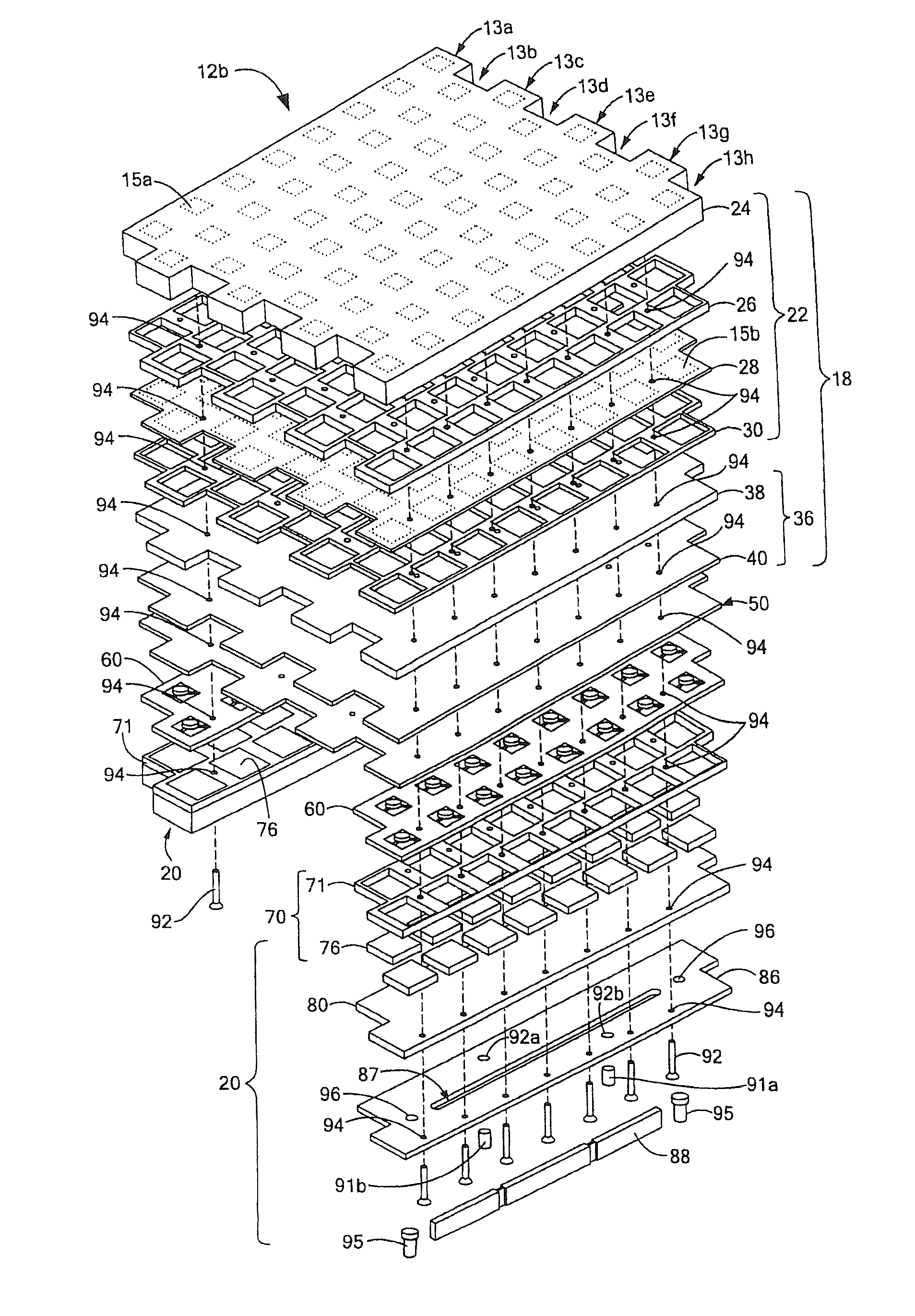
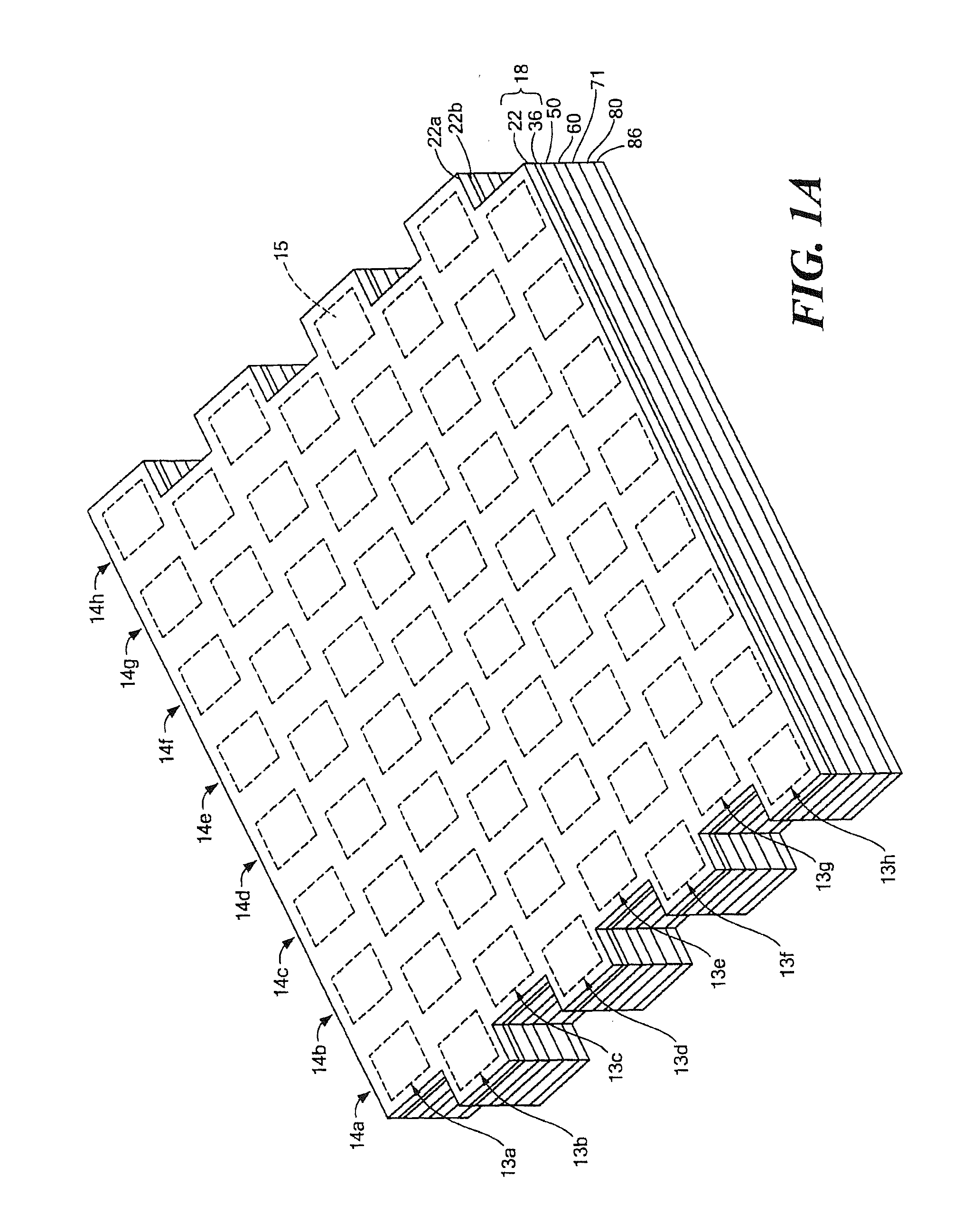
[0076]Before describing the various embodiments of the invention, some introductory concepts and terminology are explained. A “panel array” (or more simply “panel) refers to a multilayer printed wiring board (PWB) which includes an array of antenna elements (or more simply “radiating elements” or “radiators”), as well as RF, logic and DC distribution circuits in one highly integrated PWB. A panel is also sometimes referred to herein as a tile array (or more simply, a “tile”).

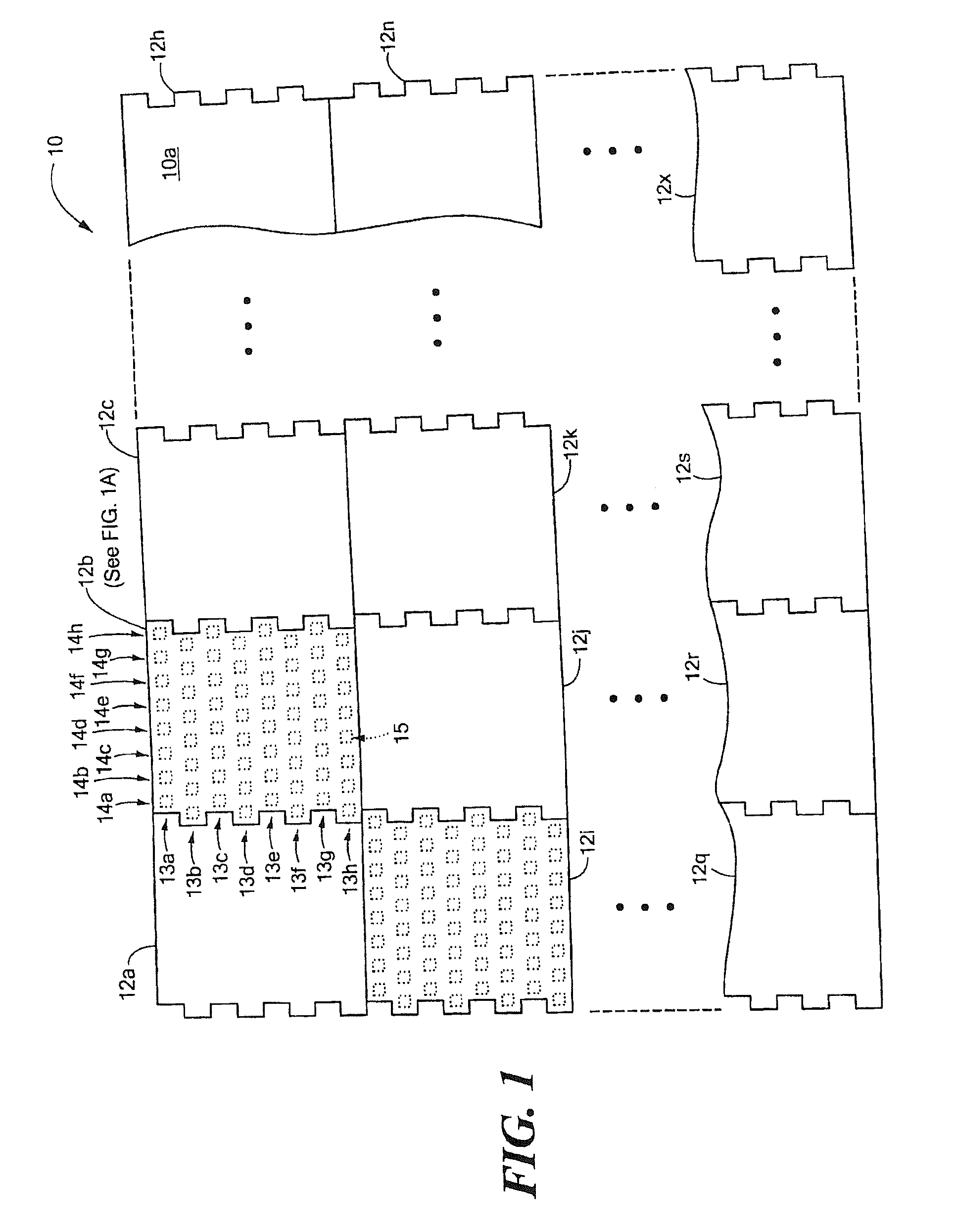
[0077]An array antenna may be provided from a single panel (or tile) or from a plurality of panels. In the case where an array antenna is provided from a plurality of panels, a single one of the plurality of panels is sometimes referred to herein as a “panel sub-array” (or a “tile sub-array”).

[0078]Reference is sometimes made herein to an array antenna having a particular number of panels. It should of course, be appreciated that an array antenna may be comprised of any number of panels and that one of ordinary ...


PUM

PropertyMeasurementUnit
thickaaaaaaaaaa
frequenciesaaaaaaaaaa
frequencyaaaaaaaaaa

Abstract

A mixed-signal, multilayer printed wiring board fabricated in a single lamination step is described. The PWB includes one or more radio frequency (RF) interconnects between different circuit layers on different circuit boards which make up the PWB. The PWB includes a number of unit cells with radiating elements and an RF cage disposed around each unit cell to isolate the unit cell. A plurality of flip-chip circuits are disposed on an external surface of the PWB and a heat sink can be disposed over the flip chip components.

Description

CROSS-REFERENCE TO RELATED APPLICATIONS[0001]This application is a continuation-in-part of co-pending application Ser. No. 11 / 558,126 filed on Nov. 9, 2006 which is a Divisional of application Ser. No. 11 / 533,848 filed on Sep. 21, 2006, now U.S. Pat. No. 7,348,932.FIELD OF THE INVENTION[0002]This invention relates generally to phased array antennas adapted for volume production at a relatively low cost and having a relatively low profile and more particularly to radio frequency (RF) circuits and techniques utilized in phased array antennas.BACKGROUND OF THE INVENTION[0003]As is known in the art, there is a desire to lower acquisition and life cycle costs of radio frequency (RF) systems which utilize phased array antennas (or more simply “phased arrays”). At the same time, bandwidth, polarization diversity and reliability requirements of such systems become increasingly more difficult to meet.[0004]As is also known, one way to reduce costs when fabricating RF systems is to utilize pr...

Claims


Application Information

Patent Timeline
Patent Type & Authority Applications(United States)
IPC IPC(8): H01Q21/00H01P11/00
CPCH01Q1/02H01Q9/0414H01Q21/00Y10T29/49018H01Q21/0087H01Q21/065H01Q21/0025
Inventor PUZELLA, ANGELO M.LICCIARDELLO, JOSEPH A.DUPUIS, PATRICIA S.FRANCIS, JOHN B.KOMISAREK, KENNETH S.BOZZA, DONALD A.ALM, ROBERTO W.
Owner RAYTHEON CO
Why Eureka
Try Eureka