Efficient fault tolerance method for nano CMOS (Complementary Metal-Oxide-Semiconductor Transistor) circuit capable of effectively utilizing normally-closed defect unit

A normally closed, defect technology, applied in CAD circuit design, nanotechnology CAD, electrical digital data processing and other directions, can solve the problems of low utilization, poor solution quality, slow mapping speed, etc., to optimize performance and simplify fault tolerance. difficulty, and the effect of improving the success rate of mapping

Active Publication Date: 2020-02-25
NINGBO UNIV
View PDF5 Cites 0 Cited by
  • Summary
  • Abstract
  • Description
  • Claims
  • Application Information

AI Technical Summary

Problems solved by technology

[0007] The technical problem to be solved by the present invention is to address the problems of low utilization rate of defective units, poor solution quality, and slow mapping speed in the fault-tolerant process of normally closed defects in the existing mapping method. Next, provide an efficient fault-tolerant method for nano-CMOS circuits that effectively utilizes normally closed defect cells

Method used


Image

  • Efficient fault tolerance method for nano CMOS (Complementary Metal-Oxide-Semiconductor Transistor) circuit capable of effectively utilizing normally-closed defect unit
  • Efficient fault tolerance method for nano CMOS (Complementary Metal-Oxide-Semiconductor Transistor) circuit capable of effectively utilizing normally-closed defect unit
  • Efficient fault tolerance method for nano CMOS (Complementary Metal-Oxide-Semiconductor Transistor) circuit capable of effectively utilizing normally-closed defect unit

Examples


Embodiment 1

[0055] Embodiment 1: Taking the s27 circuit in the ISCAS'89 reference circuit as an example, the sequence diagram of the original input signal is shown.

[0056] Figure 4 In the shown ISCAS'89 logic circuit structure, there are 7 original input signals and 8 layers of logic levels. The dotted line marks the critical path. It can be seen that the critical path contains 1 original input signal i 5 , 9 gate nodes. Only i is input among the 7 original input signals 1 The signal is not transmitted to the critical path node. right Figure 4 The raw input signal sequencing method for the logic circuit shown consists of the following steps:

[0057] Step ①: From logic level 1 (eg Figure 4 As shown in L1 in ), search for the original input signal located at the key node in the logic level, arrange the original input signal next to the sorted original input signal, such as node g in L1 11 , whose original input signal is i 5 , the key node g in L2 16 has two input signals: g ...

Embodiment 2

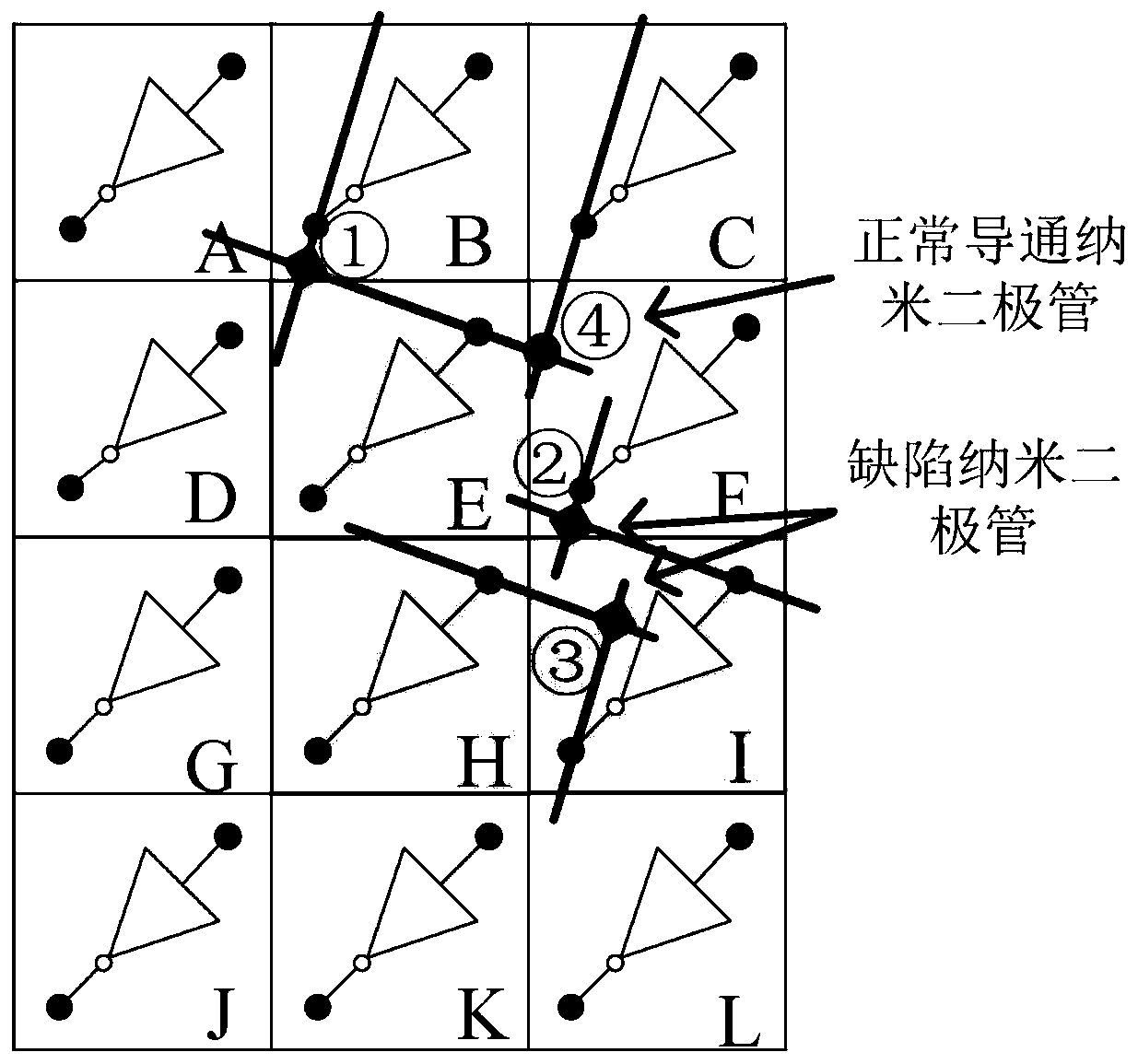
[0063] Example 2: Will Figure 5 A simple circuit with three inputs and one output is shown hierarchically mapped to Image 6 In the shown 4×3 nanometer CMOS circuit, the utilization of normally-off defective cells is performed.

[0064] When the radius of the connected domain of the nano-CMOS circuit is r=2, the size of the connected domain of the nano-CMOS unit is 4, that is, any nano-CMOS unit can realize logic functions within the range of four nano-CMOS units up, down, left, and right. Will Figure 5 The three inputs of the simple circuit shown are respectively mapped on the nano-CMOS units B, F, and D, among which B and F will become the sequential inputs of the normally-closed defect units E and I through the nano-diodes ① and ② with normally-off defects, respectively. At the same time, the normally closed defect unit I will become the sequential input unit of the normally closed defect unit H through the nanodiode ③ with normally closed defects.

[0065] Using the n...

Embodiment 3

[0072] Example 3: In such as Figure 7 Shown r=2, in the nanometer CMOS circuit of 4*3 size pair Figure 5 A simple circuit with three inputs and one output is shown for high-efficiency fault tolerance.

[0073] Figure 7 The connected domain size of the shown nanometer CMOS circuit is 4, and the Figure 5 The three inputs of the simple circuit shown are respectively mapped on nanometer CMOS cells A, C, and F, and the gate node g 1 and g 2 Has been mapped on the nanometer CMOS unit B, I respectively. The nano-CMOS unit B becomes the sequential input unit of the normally-closed defect unit E through the normally-closed defect nano-diode ①. Gate node g to be mapped 3 The input gate node g of 1 and g 2 The mapped nanometer CMOS cells B and I have no intersection of connected domains.

[0074] exist Figure 7 Defects shown in nanometer CMOS circuits for Figure 5 Gate node g shown 3 The process of mapping and fault tolerance of the overall circuit includes the followin...


PUM


Abstract

The invention discloses an efficient fault tolerance method for a nano CMOS (Complementary Metal-Oxide-Semiconductor Transistor) circuit capable of effectively utilizing a normally-closed defect unit.The connection relationship between the sequence input unit and the normally closed defect unit is matched with the logic relationship between nodes in the logic circuit; the normally-closed defect unit is used for mapping of logic nodes of all levels. Meanwhile, the defect information of the nano CMOS circuit is considered in the initial mapping process; the hierarchical mapping of the logic circuit fully considers the logic relationship between the gate nodes, the local optimization result is synthesized, the tabu search algorithm with strong local search capability is adopted to verify thefunctional correctness of the unit mapped by each logic level node, and the practical process of the nano CMOS circuit structure is accelerated. According to the invention, the mapping success rate is improved by using the available normally-closed defect units, the performance of the mapped nano CMOS circuit is optimized, the fault-tolerant complexity of the circuit is simplified, and the influence of the normally-closed defects on the logic function of the nano CMOS circuit is quickly eliminated under the condition of improving the unit utilization rate and the mapping success rate.

Description

technical field [0001] The invention relates to the field of integrated circuits, in particular to a high-efficiency fault-tolerant method for nanometer CMOS circuits that effectively utilizes normally closed defect units. Background technique [0002] The narrowing of the line width of the manufacturing process has made the traditional silicon-based CMOS integrated circuits enter the nanoscale size, and many technical difficulties have arisen, such as: the continuous increase in manufacturing costs, and the impact of microscopic quantum effects on signal integrity, etc., making people It is hoped that the new process technology can meet the needs of current development. In recent years, the development of emerging nanoelectronic devices and corresponding hybrid circuits based on nano-devices has been able to provide circuits with higher integration density and operating frequency. Among them, in 2005, Likharev and his colleagues proposed a CMOS / nanowire / MOLecular hybrid (C...

Claims


Application Information

Patent Timeline
Patent Type & Authority Applications(China)
IPC IPC(8): G06F30/398G06F30/3308G06F117/02G06F111/14
Inventor 夏银水查晓婧
Owner NINGBO UNIV
Why Eureka
Try Eureka