Quantum chip package device

A chip packaging and quantum technology, applied in electrical components, magnetic field/electric field shielding, screening enclosures, etc., can solve problems such as affecting the shielding effect, unable to achieve static magnetic field shielding, and unable to effectively ensure the working environment of the quantum chip to be packaged. Good adhesion effect, ensuring the effect of electromagnetic shielding effect

Active Publication Date: 2018-12-07
ORIGIN QUANTUM COMPUTING TECH (HEFEI) CO LTD
View PDF12 Cites 0 Cited by
  • Summary
  • Abstract
  • Description
  • Claims
  • Application Information

AI Technical Summary

Problems solved by technology

[0004] In this prior art, only a shielding barrel structure made of aluminum alloy 6061 is used as the packaging box structure for magnetic field radiation noise. When this structure is used, it can only realize the shielding of electromagnetic radiation noise, and cannot realize the shielding including static magnetic field.
In addition, coating the infrared radiation shielding layer on the inner wall of the shielding bucket in this publication will have a negative impact on the skin effect of electromagnetic shielding on the inner surface of the shielding bucket, thereby affecting the shielding effect, and cannot effectively ensure the working environment of the quantum chip to be packaged.

Method used


Image

  • Quantum chip package device
  • Quantum chip package device
  • Quantum chip package device

Examples


Embodiment Construction

[0053] The embodiments described below by referring to the figures are exemplary only for explaining the present invention and should not be construed as limiting the present invention.

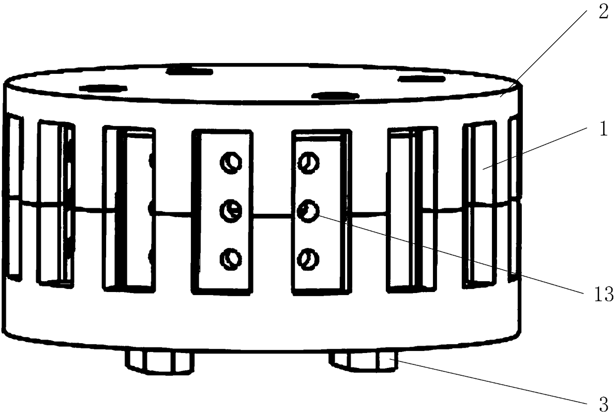
[0054] Embodiments of the present invention provide a quantum chip packaging device, please refer to figure 1 As shown, the quantum chip packaging device includes an electromagnetic shielding packaging box 1 and a static magnetic shielding cover 2 .

[0055] Wherein: the electromagnetic shielding packaging box 1 is used to place quantum chips to be packaged horizontally, and the electromagnetic shielding packaging box 1 has an electromagnetic shielding effect; the static magnetic shielding cover 2, the static magnetic shielding cover 2 is wrapped in the electromagnetic shielding packaging box 1, and the magnetostatic shield 2 has a magnetostatic shielding effect.

[0056] Facing the requirements of the harsh working environment of the quantum chip, the present invention provides a quantum ch...


PUM


Abstract

The present invention belongs to the field of chip package, and especially discloses a quantum chip package device. The quantum chip package device comprises: an electromagnetic shielding package boxconfigured to horizontally putting a quantum chip to be packaged and having an electromagnetic shielding effect; and a magnetostatic shielding cover coating the external portion of the electromagneticshielding package box and having a magnetostatic shielding effect. For the demand for the severe work environment of the quantum chip, the present invention provides a quantum chip package device with two layers of shielding structures, wherein the two layers of shielding structures are the electromagnetic shielding package box having the electromagnetic shielding effect and the magnetostatic shielding cover having the magnetostatic shielding effect coating the external portion of the electromagnetic shielding package box, the layers of the shielding structures work together to achieve shielding of different types of magnetic fields and magnetic fields with different intensities so as to commonly guarantee the work environment of the quantum chip to be packaged in the electromagnetic shielding package box.

Description

technical field [0001] The invention belongs to the technical field of chip packaging, in particular to a quantum chip packaging device. Background technique [0002] The three-dimensional packaging technology is widely used in the packaging of quantum chips because it can lead out the signal on the quantum chip through the third vertical dimension. It can accommodate more quantum elements without expanding the size of the quantum chip, and at the same time , the size of the packaging box can be reasonably adjusted according to the size of the quantum chip, so that the redundant space around the quantum chip can be compressed as much as possible, the spatial standing wave mode can be improved, and the interference between the spatial standing wave and the quantum element can be avoided. [0003] Due to the harsh working conditions of the quantum chip, a good working environment such as extremely low working temperature and effective noise shielding is required. In the prior ...

Claims


Application Information

Patent Timeline
Patent Type & Authority Applications(China)
IPC IPC(8): H05K9/00
CPCH05K9/0007
Inventor 高峰李松孔伟成
Owner ORIGIN QUANTUM COMPUTING TECH (HEFEI) CO LTD
Why Eureka
Try Eureka