Check patentability & draft patents in minutes with Patsnap Eureka AI!

PHY interface and FPGA chip based on FPGA primitive

An interface and chip technology, applied in the field of FPGA, can solve the problems of long delay period of PHY interface and inability to dynamically configure delay parameters.

Active Publication Date: 2018-12-11
ZHENGZHOU YUNHAI INFORMATION TECH CO LTD
View PDF7 Cites 5 Cited by
  • Summary
  • Abstract
  • Description
  • Claims
  • Application Information

AI Technical Summary

Problems solved by technology

[0004] The purpose of the present invention is to provide a kind of PHY interface and FPGA chip based on FPGA primitive, in order to solve the problem that traditional PHY interface delay period is long, can not dynamically configure the delay parameter

Method used


Image

  • PHY interface and FPGA chip based on FPGA primitive
  • PHY interface and FPGA chip based on FPGA primitive
  • PHY interface and FPGA chip based on FPGA primitive

Examples


Embodiment Construction

[0023] The core of the invention is to provide a PHY interface and FPGA chip based on FPGA primitives, which improves the flexibility of the PHY interface and reduces the data transmission delay of the PHY interface.

[0024] In order to enable those skilled in the art to better understand the solution of the present invention, the present invention will be further described in detail below in conjunction with the accompanying drawings and specific embodiments. Apparently, the described embodiments are only some of the embodiments of the present invention, but not all of them. Based on the embodiments of the present invention, all other embodiments obtained by persons of ordinary skill in the art without making creative efforts belong to the protection scope of the present invention.

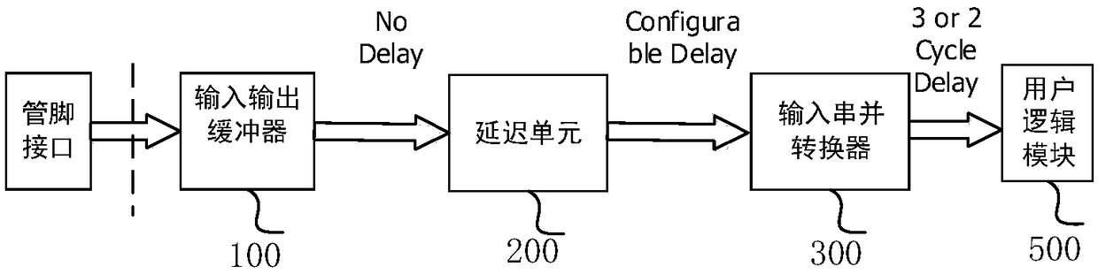
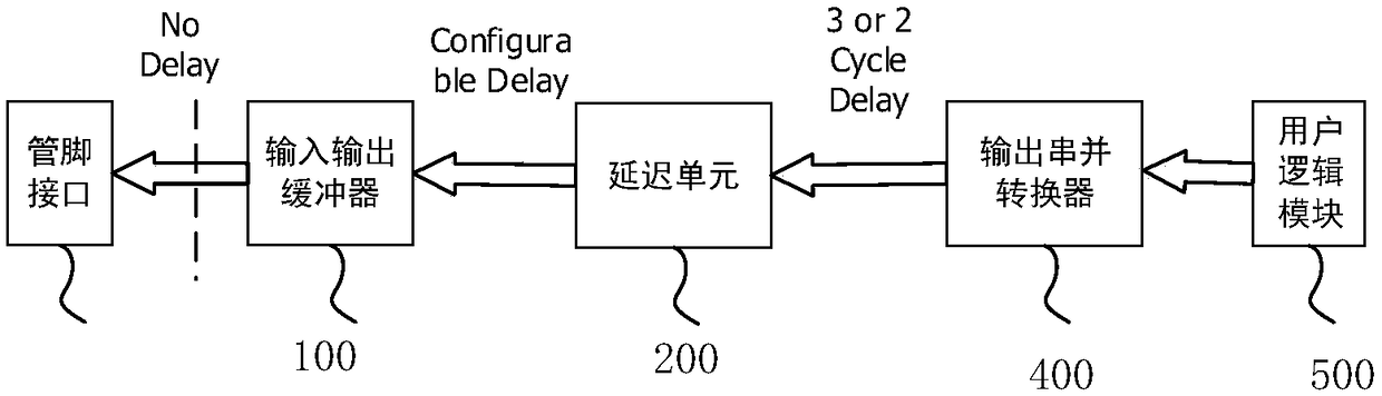
[0025] A kind of PHY interface embodiment based on FPGA primitive provided by the present invention is introduced below, see figure 1 , the example includes:

[0026] The I / O buffer 100 for bu...


PUM


Abstract

The invention discloses a PHY interface based on FPGA primitive. The PHY interface includes input and output buffers, a delay unit, an input serial-to-parallel converter and an output serial-to-parallel converter Both the input serial-to-parallel converter and the output serial-to-parallel converter are connected to a user logic block, the input serial-to-parallel converter and the output serial-to-parallel converter are both provided with an input interface clock and a frequency dividing clock, and the user logic module can adjust the phase difference between the input interface clock and thefrequency dividing clock to change the data transmission delay of the PHY interface. The inherent delay of the PHY interface realized by FPGA primitive is low and data transmission delay can be adjusted by adjusting clock of user logic module, flexibility of PHY interface is improved and data transmission delay of PHY interface is reduced. The invention also provides an FPGA chip, the function ofwhich corresponds to the PHY interface.

Description

technical field [0001] The invention relates to the FPGA field, in particular to a PHY interface and an FPGA chip based on FPGA primitives. Background technique [0002] PHY is the physical layer, and the PHY interface refers to the physical layer interface for data transmission between chip-to-chip or circuit board-to-circuit board. For example, in Ethernet applications, Ethernet data must pass through the PHY interface chip and then be transmitted to the CPU; on FPGA-based application platforms, FPGA control and data signals must pass through the high-speed PHY interface and then be transmitted to peripheral PCIe devices or DDR4 on the memory stick. In high-speed data applications, the PHY interface module (implemented by chips, application-specific integrated circuits or FPGA logic) is an essential part. The transmission speed and delay time of the PHY interface are important indicators to measure the interface. [0003] At present, there are dedicated PHY interface chi...

Claims


Application Information

Patent Timeline
IPC IPC(8): G06F13/38G06F13/42
CPCG06F13/382G06F13/4221
Inventor 任智新
Owner ZHENGZHOU YUNHAI INFORMATION TECH CO LTD
Features
  • R&D
  • Intellectual Property
  • Life Sciences
  • Materials
  • Tech Scout
  • Unparalleled Data Quality
  • Higher Quality Content
  • 60% Fewer Hallucinations
Learn More