Pixel demarcation layer and manufacturing method thereof, and display substrate

A pixel definition layer and manufacturing method technology, applied in the direction of electrical components, electric solid devices, circuits, etc., can solve the problems of low structural stability of the pixel definition layer, complex preparation process of the pixel definition layer, etc., to improve production efficiency and structure Stability, the effect of simplifying the preparation process

Active Publication Date: 2018-12-11
BOE TECH GRP CO LTD
View PDF5 Cites 14 Cited by
  • Summary
  • Abstract
  • Description
  • Claims
  • Application Information

AI Technical Summary

Problems solved by technology

[0006] Embodiments of the present invention provide a pixel defining layer, a manufacturing method thereof, and a display substrate, which can solve the problems of low structural stability of the pixel defining layer and complicated preparation process of the pixel defining layer in the related art

Method used


Image

  • Pixel demarcation layer and manufacturing method thereof, and display substrate
  • Pixel demarcation layer and manufacturing method thereof, and display substrate
  • Pixel demarcation layer and manufacturing method thereof, and display substrate

Examples


Embodiment Construction

[0035] In order to make the object, technical solution and advantages of the present invention clearer, the implementation manner of the present invention will be further described in detail below in conjunction with the accompanying drawings.

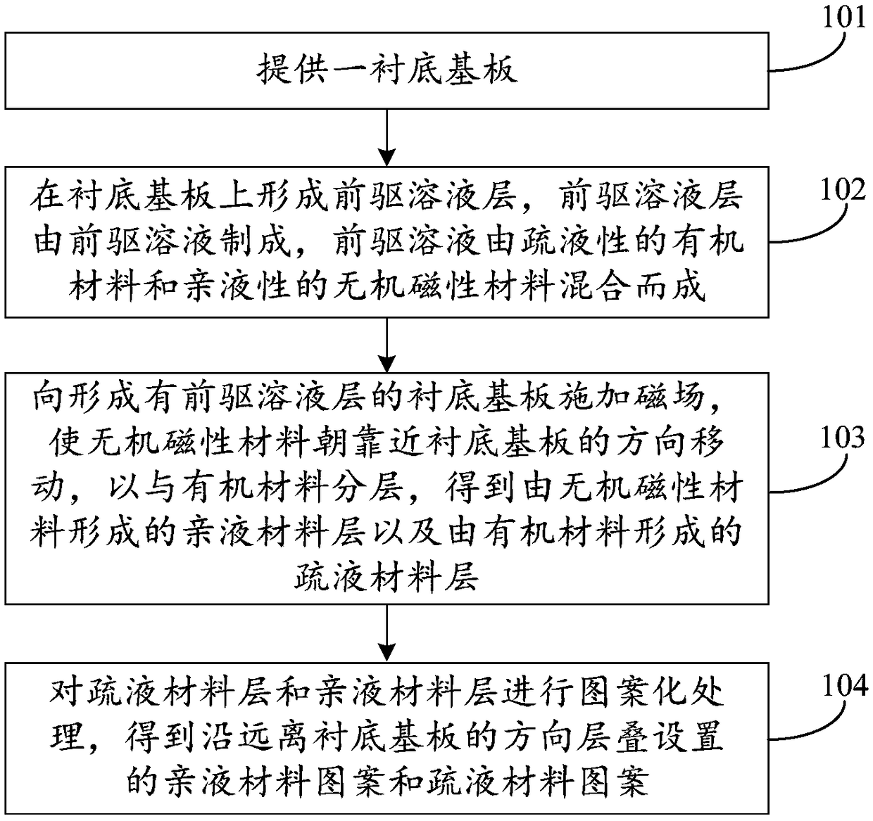
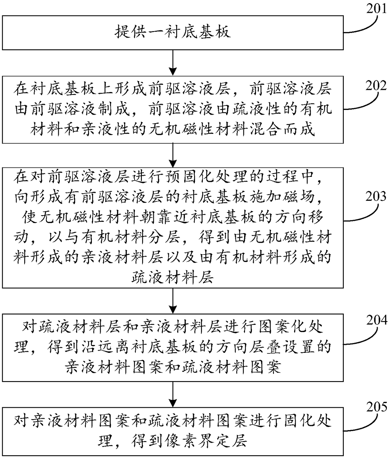
[0036] figure 1 It is a flowchart of a method for manufacturing a pixel defining layer provided by an embodiment of the present invention, as shown in figure 1 As shown, the method includes:

[0037] Step 101, providing a base substrate.

[0038] Step 102 , forming a precursor solution layer on the base substrate. The precursor solution layer is made of a precursor solution, and the precursor solution is a mixture of a lyophobic organic material and a lyophilic inorganic magnetic material.

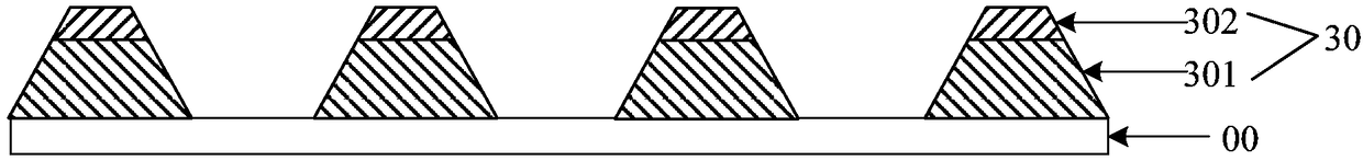
[0039] Step 103, applying a magnetic field to the base substrate on which the precursor solution layer is formed, so that the inorganic magnetic material moves toward the direction close to the base substrate, so as to be layered with the organic...


PUM

PropertyMeasurementUnit
thicknessaaaaaaaaaa
thicknessaaaaaaaaaa
thicknessaaaaaaaaaa

Abstract

The invention discloses a pixel demarcation layer and a manufacturing method thereof and a display substrate, belongs to the technical field of display. The manufacturing method of the pixel demarcation layer includes providing a substrate substrate; Forming a precursor solution layer on the substrate, wherein the precursor solution layer is made of a precursor solution, and the precursor solutionis formed by mixing a hydrophobic organic material and a hydrophilic inorganic magnetic material; Applying a magnetic field to a substrate on which the precursor solution layer is formed to obtain ahydrophilic material layer formed of the inorganic magnetic material and a hydrophobic material layer formed of the organic material; The liquid-repellent material layer and the liquid-repellent material layer are patterned to obtain a liquid-repellent material pattern and a liquid-repellent material pattern stacked in a direction away from the substrate. The invention simplifies the preparation process of the pixel bounding layer, improves the production efficiency of the pixel bounding layer, and improves the structural stability of the pixel bounding layer. The present invention is used tofabricate a pixel bounding layer.

Description

technical field [0001] The invention relates to the field of display technology, in particular to a pixel defining layer, a manufacturing method thereof, and a display substrate. Background technique [0002] A self-illuminating display panel generally includes a base substrate and an anode, a light-emitting layer, a cathode, and the like disposed on the base substrate in sequence. Wherein, the light emitting layer generally includes a hole injection layer, a hole transport layer, a light emitting material layer, an electron transport layer and an electron injection layer. Each film layer in the light-emitting layer can be prepared by ink-jet printing (Ink-Jet Printing, IJP) technology. Before using the inkjet printing technology to prepare the light-emitting layer, it is necessary to form a pixel defining layer on the base substrate, and then sequentially spray the corresponding solution onto the base substrate on which the pixel defining layer is formed, so as to form eac...

Claims


Application Information

Patent Timeline
Patent Type & Authority Applications(China)
IPC IPC(8): H01L27/32
CPCH10K59/122H10K59/1201
Inventor 姜博靳倩黄美燕
Owner BOE TECH GRP CO LTD
Why Eureka
Try Eureka