A preparation method of a printing thimble template and a printing thimble template

A production method and technology of thimbles, which are applied in the fields of printed circuit manufacturing, printed circuits, printed circuits assembled with electric components, etc., can solve the problems of inaccurate layout position, low efficiency of thimbles, and low product reliability, and solve the problem of easy concentration of stress , Improve work efficiency and improve reliability

Active Publication Date: 2018-12-11
CHANGSHA GREE HVAC EQUIP CO LTD +1
View PDF5 Cites 4 Cited by
  • Summary
  • Abstract
  • Description
  • Claims
  • Application Information

AI Technical Summary

Problems solved by technology

[0004] Therefore, the technical problem to be solved by the present invention is to overcome the low efficiency of manually arranging thimbles when switching lines in the PCB board preparation process, and the defects of low product reliability caused by inaccurate layout positions

Method used


Image

  • A preparation method of a printing thimble template and a printing thimble template
  • A preparation method of a printing thimble template and a printing thimble template
  • A preparation method of a printing thimble template and a printing thimble template

Examples


Embodiment 1

[0056] This embodiment provides a method for making a printing thimble template in the present invention, which specifically includes:

[0057] S1. Confirm that the first layout position on the PCB is consistent with the distribution of ejector pins;

[0058] S2. Perform stress simulation on the first arrangement position, select a second arrangement position, and arrange several thimbles under the second arrangement position.

[0059] In step S1, the process of determining the first arrangement position is as follows:

[0060] First determine the thickness of the PCB board, set the thickness of the PCB board as b, and the connection distance between two adjacent and nearest thimbles as c, and then the thimble layout needs to meet:

[0061] When 0mm

[0062] When 1mm

[0063] When 1.6mm

[0064] If there are many electrical components on the PCB, the value of the thimble spacing c in the actual layout is relatively large, wh...

Embodiment approach

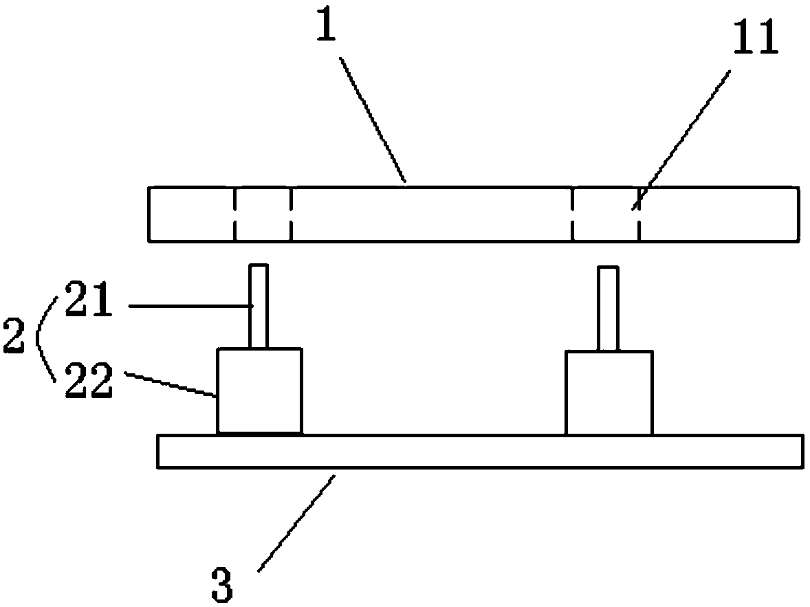
[0077] like figure 2 and 3 As shown, the present embodiment provides an implementation of the printing ejector pin template described in the present invention, including:

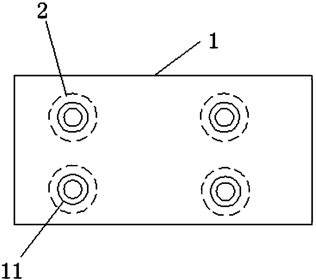
[0078] The SMT printing thimble template 1 made by the printing thimble template manufacturing method in Embodiment 1 is specifically provided with a thimble arrangement hole 11 on the PCB, and a thimble 2 is arranged directly below the thimble arrangement hole 11.

[0079] The thimble 2 in the present embodiment is formed with the supporting portion 21 of small diameter and the fixed portion 22 of large diameter, and magnetite is installed on the fixed portion 22, and the diameter of described thimble arrangement hole 11 gets final product larger than the diameter of supporting portion 21, guarantees that the worker When the thimble 2 is moved, the position of the thimble 2 can be seen through the thimble arrangement hole 11 .

[0080] During specific implementation, when switching lines in the PCB boar...

Embodiment 3

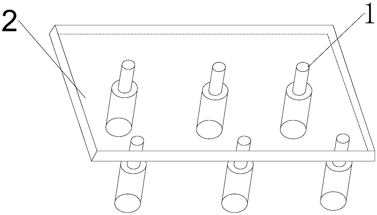
[0082] like Figure 4 and 5 As shown, this embodiment provides the second implementation of the printing thimble template in the present invention.

[0083] Compared with Embodiment 2, this embodiment is applicable to another structure of the thimble 2, and the thimble 2 is a cylinder with a certain length.

[0084] SMT printing thimble template 1, on which according to the manufacturing method of printing thimble template in the present invention, a thimble arrangement hole 11 is opened, and a thimble 2 is arranged directly under the thimble arrangement hole 11, and the diameter of the thimble arrangement hole 11 is larger than the above-mentioned The diameter of thimble 2.

[0085] During specific implementation, when switching lines in the PCB board printing solder paste process, first install the SMT printing thimble template 1 on the position of the PCB board to be printed, according to the position of the thimble hole 11 on the SMT printing thimble template 1 , holdin...


PUM

PropertyMeasurementUnit
Diameteraaaaaaaaaa

Abstract

The invention provides a manufacturing method of a printed thimble template, comprising the following steps: S1. confirming a first arrangement position on a PCB board consistent with the thimble distribution; S2. Stress simulation is performed on the first arrangement position, a second arrangement position is selected, a plurality of thimbles are arranged below the second arrangement position, and a printing thimble template produced according to the printing thimble template method is provided. The invention relates to a printing thimble stencil making method, the pre-fabricated printed thimble template is one-to-one matched with the PCB board to be printed, In addition, the position of the thimble arrangement on the PCB in the invention has accurately measured the stress and strain amount thereof, effectively preventing the damage of components or solder joints on the PCB caused by the printing process, and improving the reliability of the product.

Description

technical field [0001] The invention relates to the field of surface assembly technology, in particular to a method for preparing a printed thimble template and a printed thimble template. Background technique [0002] In SMT (Surface Mounting Technology abbreviation: Surface Mounting Technology), in the automatic printing solder paste process, such as figure 1 As shown, the PCB board 1 is easily deformed under the pressure of the scraper, causing the electrical components and solder joints on it to be damaged and cracked. In the prior art, the thimble 2 is arranged under the PCB 1 to reduce its deformation, and the position of the thimble 2 must be confirmed one by one to ensure that the thimble 2 does not interfere with the bottom surface components while avoiding the component mounting holes and the position of the fire pit. Different PCB boards 1 correspond to different arrangements of thimbles. [0003] When switching lines, the existing technical solution is to manua...

Claims


Application Information

Patent Timeline
IPC IPC(8): H05K3/30H05K3/00
CPCH05K3/0008H05K3/30
Inventor 吴品王晓彬周锴古湘龙周艳彬方掩陈烔
Owner CHANGSHA GREE HVAC EQUIP CO LTD
Why Eureka
Try Eureka