

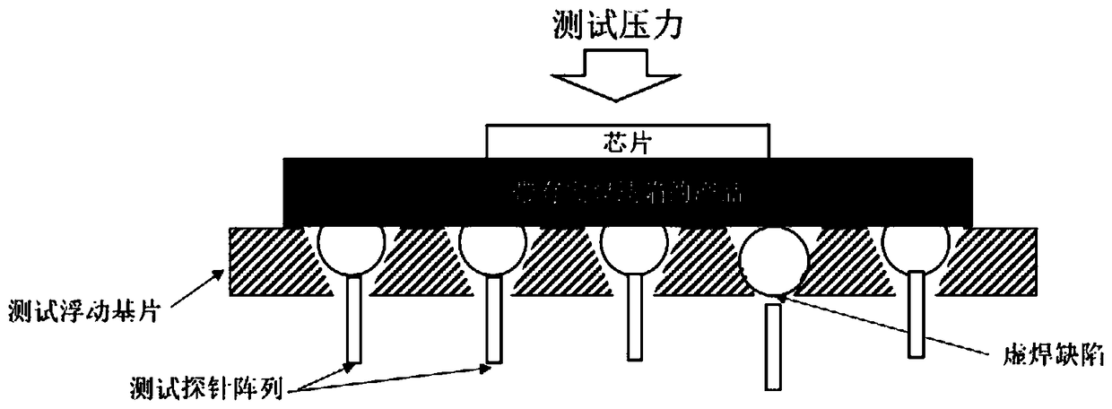
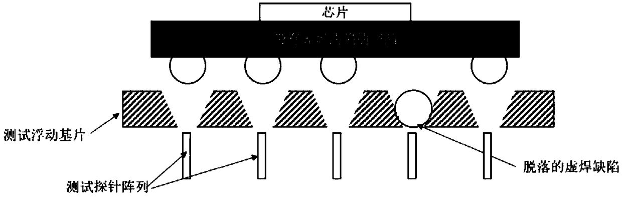
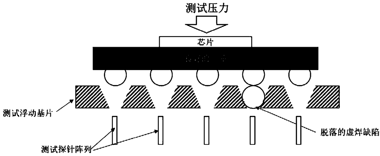
Floating base substrate for chip semiconductor testing
A semiconductor and pedestal technology, applied in the field of floating pedestal substrates for chip semiconductor testing, can solve problems such as delays, inability to really solve virtual solder damage, and affect the quality of chip units.
- Summary
- Abstract
- Description
- Claims
- Application Information
AI Technical Summary
Problems solved by technology
Method used
Image

Examples
Embodiment 1
[0069] Example 1: For Product A
[0070]
[0071] Conclusion: For product A whose original design does not meet design criterion 1 or design criterion 2, the defect of virtual soldering will cause continuous damage to the subsequent test product, and the damage will reach the scrapping standard of visual inspection after packaging. False soldering defects will damage all the good products in the follow-up test and the damage will reach the scrapping standard, which will have a considerable impact on the yield rate; according to the characteristics of the product and various boundary conditions allowed by the test hardware (R to bo s <=450μm) use the inventive model to calculate the optimal solution as shown in the table. The original design has a 100% impact on the yield rate in the case of false welding defects, that is, all subsequent test products will be damaged and the damage reaches the scrap standard; the improved design is actually used in the case of false welding ...
Embodiment 2
[0072] Example 2: For Product B
[0073]
[0074] Conclusion: For product B whose original design does not meet design criterion 1 or design criterion 2, the defect of solder joints will cause continuous damage to the subsequent test product, and the damage will reach the scrapping standard of visual inspection after packaging. False soldering defects will damage all the good products in the follow-up test and the damage will reach the scrap standard, which will have a considerable impact on the yield rate; according to the characteristics of the product and various boundary conditions allowed by the test hardware (R to bo s bo and H s Do proper optimization. The original design has a 100% impact on the yield rate in the case of false welding defects, that is, all subsequent test products will be damaged and the damage reaches the scrap standard; the improved design is actually used in the case of false welding defects, and it is found that its The resulting yield impact ...
PUM
 Abstract
Description
Claims
Application Information