Packaging method

A packaging method and packaging layer technology, applied in the direction of electrical components, semiconductor/solid-state device manufacturing, circuits, etc., can solve the problems of packaging structure yield and reliability to be improved, so as to shorten the processing cycle, improve yield and reliability , Reduce the effect of lateral impact force

Active Publication Date: 2018-12-14
NINGBO SEMICON INT CORP
View PDF14 Cites 7 Cited by
  • Summary
  • Abstract
  • Description
  • Claims
  • Application Information

AI Technical Summary

Problems solved by technology

[0004] However, the yield and reliability of the packaging structure formed by the current packaging method still need to be improved.

Method used


Image

  • Packaging method
  • Packaging method
  • Packaging method

Examples


Embodiment Construction

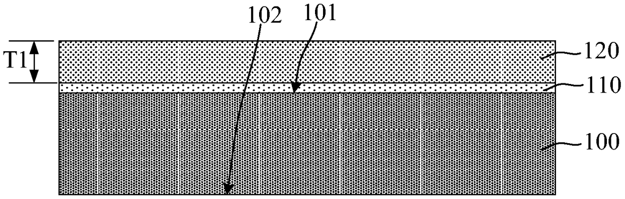
[0025] It can be seen from the background art that the yield and reliability of the packaging structure formed by the current packaging method still need to be improved. The reasons for analyzing the yield and reliability of the packaging structure to be improved are:

[0026] In the current packaging process, compared with the bonding process, the bonding process has better adhesion and chemical stability, so the bonding process has gradually become the main means to achieve wafer-level system packaging and panel-level system packaging.

[0027] However, wafer-level system package or panel-level system package is to bond chips one by one to wafers or other substrates. Due to the large number of chips, in order to shorten the processing cycle of the packaging process, the bonding time is required to be short , and the shorter bonding time will reduce the bonding strength between the chip and the wafer or other substrates; when the encapsulation layer is formed by the subsequen...


PUM

PropertyMeasurementUnit
Thicknessaaaaaaaaaa

Abstract

A packaging method includes providing a substrate, wherein a surface to be bonded of the substrate is a first surface to be bonded; providing a plurality of chips, wherein surfaces to be bonded of thechips are second surfaces to be bonded; providing a thin film type packaging materials; forming a bonding layer on at least one of the first surface to be bonded and the second surfaces to be bonded;after forming the bonding layers on at least one of the first surface to be bonded and the second surfaces to be bonded, arranging the first surface to be bonded and the second surfaces to be bondedoppositely and placing the chips on the substrate; after the chip is placed on the substrate, adopting a thermocompression bonding process to realize bonding of the substrate and the plurality of chips through the bonding layer, and filling a packaging material between the chips and the substrate and covering the chip, and using the packaging material after the thermocompression bonding process asa packaging layer. Through the thin film type packaging material, the probability of chip drift in the thermocompression bonding process is reduced, and the yield and reliability of the packaging structure are improved. Moreover, the bonding between the substrate and the chips is realized synchronously by the thermocompression bonding process, and the packaging efficiency is improved.

Description

technical field [0001] The invention relates to the field of semiconductor manufacturing, in particular to a packaging method. Background technique [0002] With the development trend of very large scale integrated circuits, the feature size of integrated circuits continues to decrease, and people's requirements for packaging technology of integrated circuits continue to increase accordingly. Among them, the system-in-package (System in Package, SIP) is to combine multiple active components, passive components, micro-electromechanical systems (MEMS), optical components and other components with different functions into one unit to form a A system or subsystem that provides multiple functions, allowing integration of heterogeneous ICs. Compared with System-on-Chip (SoC), the integration of System-in-Package is relatively simple, the design cycle and market cycle are shorter, the cost is lower, and more complex systems can be realized. It is a relatively common packaging tech...

Claims


Application Information

Patent Timeline
IPC IPC(8): H01L21/56H01L21/60
CPCH01L21/568H01L21/563
Inventor 石虎刘孟彬
Owner NINGBO SEMICON INT CORP
Why Eureka
Try Eureka