Packaging method

一种封装方法、封装层的技术,应用在电气元件、半导体/固态器件制造、电路等方向,能够解决封装结构良率和可靠性有待提高等问题

Inactive Publication Date: 2022-02-15
NINGBO SEMICON INT CORP
View PDF0 Cites 0 Cited by
  • Summary
  • Abstract
  • Description
  • Claims
  • Application Information

AI Technical Summary

Problems solved by technology

[0005] However, the yield and reliability of the packaging structure formed by the current packaging method still need to be improved.

Method used


Image

  • Packaging method
  • Packaging method
  • Packaging method

Examples


Embodiment Construction

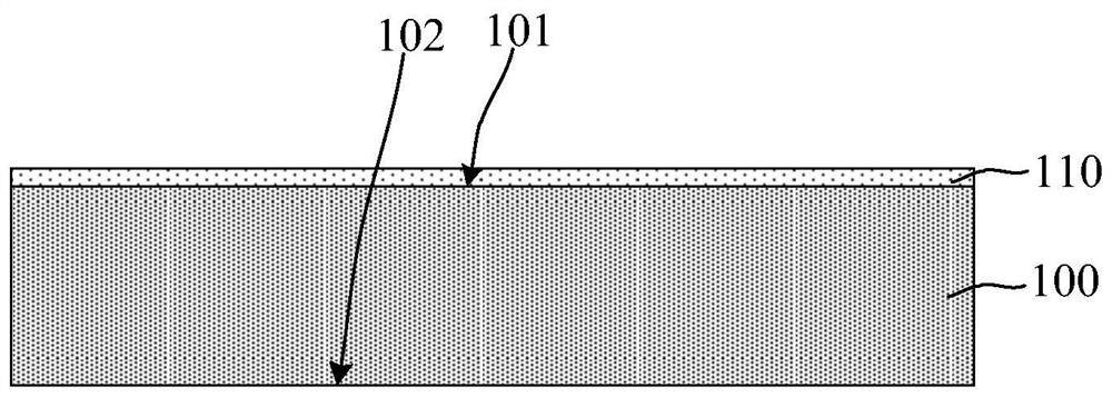
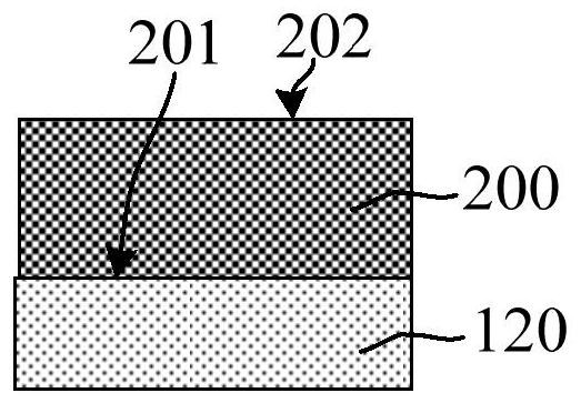
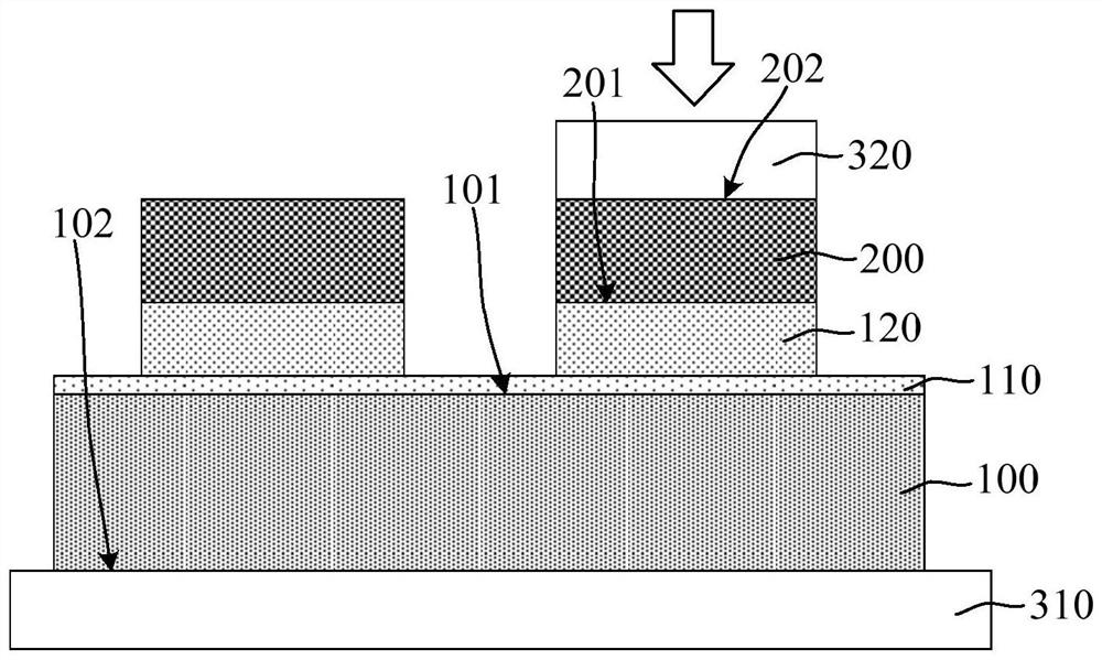
[0013] It can be seen from the background art that the yield and reliability of the packaging structure formed by the current packaging method still need to be improved. The reasons for analyzing the yield and reliability of the packaging structure to be improved are:

[0014] In the current packaging process, compared with the bonding process, the bonding process has better adhesion and chemical stability, so the bonding process has gradually become the main means to achieve wafer-level system packaging and panel-level system packaging.

[0015] However, wafer-level system package or panel-level system package is to bond chips one by one to wafers or other substrates. Due to the large number of chips, in order to shorten the processing cycle of the packaging process, the bonding time is required to be short , and the shorter bonding time will reduce the bonding strength between the chip and the wafer or other substrates; when the encapsulation layer is formed by the subsequen...


PUM


Abstract

The invention discloses a packaging method. The packaging method comprises the following steps: providing a substrate; forming an adhesive layer on the substrate; a plurality of chips are provided, and bonding layers are formed on the chips; placing the chip on the substrate, so that the bonding layer and the adhesive layer are oppositely arranged, and bonding of the chip and the substrate is achieved. Compared with a bonding layer, the bonding layer has the characteristics of higher bonding strength, good chemical resistance, acid and alkali resistance, high temperature resistance and the like, and after the bonding layer is adopted, the requirement of a bonding process on shearing force is reduced, complete bonding of the substrate and the chip can be realized within a short process time, and the drifting probability of the chip on the substrate is also relatively low.

Description

[0001] This application is a divisional application of the Chinese invention patent application with application number 201810883152.9, application date 2018.08.06, and invention name "encapsulation method". technical field [0002] The invention relates to the field of semiconductor manufacturing, in particular to a packaging method. Background technique [0003] With the development trend of very large scale integrated circuits, the feature size of integrated circuits continues to decrease, and people's requirements for packaging technology of integrated circuits continue to increase accordingly. Among them, the system-in-package (System in Package, SIP) is to combine multiple active components, passive components, micro-electromechanical systems (MEMS), optical components and other components with different functions into one unit to form a A system or subsystem that provides multiple functions, allowing integration of heterogeneous ICs. Compared with System-on-Chip (SoC...

Claims


Application Information

Patent Timeline
Patent Type & Authority Applications(China)
IPC IPC(8): H01L21/56
CPCH01L21/568H01L21/563
Inventor 石虎刘孟彬
Owner NINGBO SEMICON INT CORP
Why Eureka
Try Eureka