

Anti-ultraviolet planar light source optical structure, anti-UV diffusion layer and LED panel light
A technology of LED flat light and flat light source, applied in the field of optical structure, can solve the problems of uneven brightness, reduced brightness, discoloration and yellowing, etc., and achieve the effect of slowing down the aging speed, avoiding the reduction of brightness, and saving the cost of materials
- Summary
- Abstract
- Description
- Claims
- Application Information
AI Technical Summary
Problems solved by technology
Method used
Image

Examples
Embodiment 1
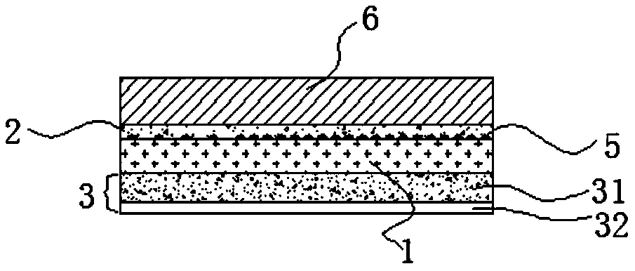
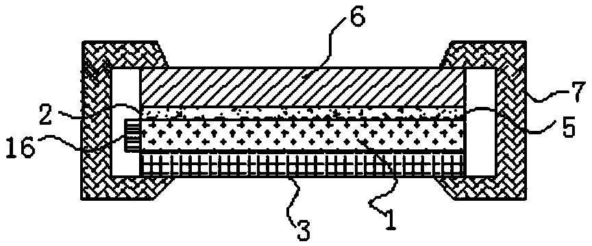
[0084] Embodiment 1: A kind of LED flat lamp that contains the above-mentioned anti-ultraviolet planar light source optical structure provided by the present invention, such as Figure 3.1 As shown, it also includes a light source 16, a back plate 6 and a frame 7, the back plate is located outside the reflective layer, the anti-ultraviolet diffusion layer, the light guide layer, the reflective layer and the back plate are all It is fixed in the outer frame, and the incident point of the light source is located at the side of the light guide layer.
Embodiment 2
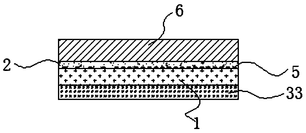
[0085] Embodiment 2: a kind of LED panel lamp, as Figure 3.2 , Figure 4 , Figure 5 , Figure 7 and Figure 8 As shown, there is also a buffer layer 4 between the back plate and the reflective layer. The structure is flat.
[0086] The cushioning layer 4 is a plastic-absorbing cushioning layer, and the blistering cushioning layer is a plastic-absorbing product formed by connecting convex parts 41 and concave parts 42, such as Figure 4 and Figure 5 As shown, the cushioning layer can also be a cushioning material of a non-absorbing product, such as a spring, EVA (ethylene-vinyl acetate copolymer) cushioning material, EPP (expanded polypropylene) cushioning material, EPE (expandable polyethylene ) cushioning material or EPO (expanded polystyrene polyethylene compound) cushioning material, but not limited thereto.
[0087] Preferably, the buffer layer 4 has a thickness of 0.3-15mm.
[0088] Described blister buffer layer is PVC (polyvinyl chloride material) layer, PET ...
Embodiment 3
[0096] Embodiment 3: a kind of LED panel lamp, such as Image 6 As shown, the light guide layer is a wedge-shaped light guide layer with a right-angled trapezoidal cross section, the thicker side of the light guide layer is the light-incoming side, and the light-incoming side is provided with LED light bars 19, and the thinner side of the light guide layer is Cushioning material 9 is provided. Wherein, the cross-section of the buffer layer or the backplane is also a right-angled trapezoid, and it only needs to ensure that the stacked structure composed of the backplane, the light guide layer, the reflective layer and the buffer layer is flat.
PUM
| Property | Measurement | Unit |
|---|---|---|
| Thickness | aaaaa | aaaaa |
Abstract
Description
Claims
Application Information