Check patentability & draft patents in minutes with Patsnap Eureka AI!

Probe manufacturing device and manufacturing method

A technology for manufacturing devices and manufacturing methods, which is applied in the field of probe manufacturing devices, can solve the problems of elongated probe thickness and difficulty in using mechanical processing methods, and achieve the effect of fast processing speed

Active Publication Date: 2020-11-03
SAE HAN MICRO TECH
View PDF16 Cites 0 Cited by
  • Summary
  • Abstract
  • Description
  • Claims
  • Application Information

AI Technical Summary

Problems solved by technology

However, there is a problem that as the distance between the pads of the semiconductor chip becomes shorter, the thickness of the probe also becomes longer, so it is difficult to use the conventional machining method

Method used


Image

  • Probe manufacturing device and manufacturing method
  • Probe manufacturing device and manufacturing method
  • Probe manufacturing device and manufacturing method

Examples


Embodiment Construction

[0028] Embodiments of the present invention will be described in detail below with reference to the accompanying drawings. However, the embodiments of the present invention can be modified into various other forms, and it cannot be interpreted that the scope of the present invention is limited by the embodiments described in detail below. The embodiments of the present invention are provided to more fully explain the present invention to those skilled in the art. Therefore, the shapes of elements in the drawings are exaggerated to emphasize clearer description, and elements denoted by the same symbols in the drawings mean the same elements.

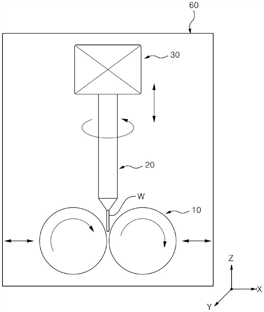
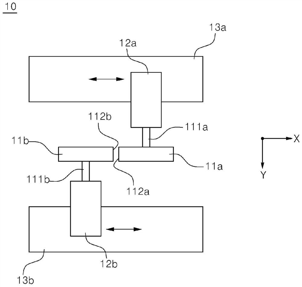
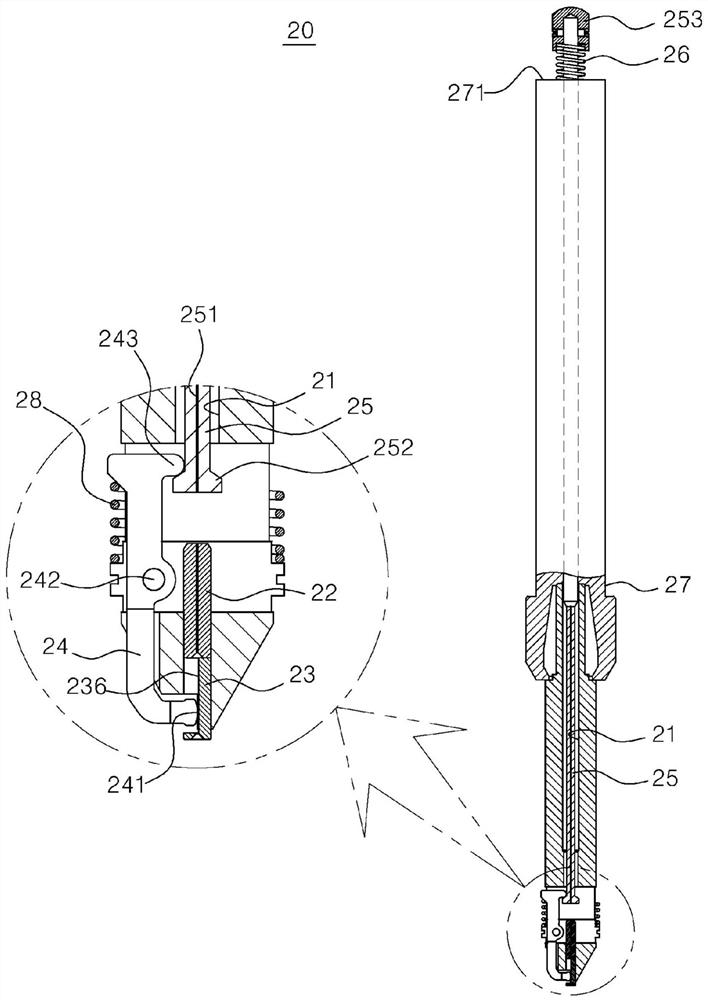
[0029] figure 1 It is a front view of an Example of the probe manufacturing apparatus of this invention. like figure 1 As shown in the figure, an embodiment of the probe manufacturing device of the present invention includes a support structure 60, a rotating grindstone part 10 provided on the support structure 60, a wire clamp 20, and...


PUM


Abstract

The present invention relates to a device and a method for manufacturing a probe pin and, more particularly, to a device and a method for manufacturing a probe pin by polishing a pointed end of a metal wire. The present invention provides a probe pin manufacturing device for manufacturing a probe pin by polishing an end of a metal wire, the probe pin manufacturing device comprising: a support structure having X-axis, Y-axis, and Z-axis directions; a pair of rotating grindstones having outer peripheral surfaces, which are polishing surfaces, arranged to face each other, each rotating grindstone having an axis of rotation parallel with the Y-axis; a grindstone transfer device installed on the support structure so as to linearly move the pair of rotating grindstones in parallel with the X-axis, thereby adjusting the interval between the pair of rotating grindstones; a wire holder installed on the support structure so as to linearly move along the Z-axis and configured to retain a wire and to rotate the same about the Z-axis as the axis of rotation; and a controller for controlling the wire holder such that the wire descends between the pair of rotating grindstones while rotating, the controller controlling the grindstone transfer device such that, as the wire descends, the interval between the pair of rotating grindstones gradually increases.

Description

technical field [0001] The present invention relates to a manufacturing device and a manufacturing method of a probe, and more specifically, to a device and a method for manufacturing a probe by grinding a tip portion of a wire. Background technique [0002] Probes are widely used to inspect the performance of semiconductor elements formed on flat panel display devices including liquid crystal display devices (Liquid Crystal Display, LCD) and plasma display panels (Plasma Display Panel, PDP), or on wafers. The probe card is used to electrically connect an inspection device (Probe Station) that performs functions required for the inspection of the object to be inspected, and the object to be inspected, and includes a collection of probes (Probe Pins) that directly contact the object to be inspected. Simple linear probes in the form of bars are simple in shape, so it is easy to manage precision, and the product reproducibility is good at the time of production. It is easy to ...

Claims


Application Information

Patent Timeline
Patent Type & Authority Patents(China)
IPC IPC(8): G01R1/067G01R3/00G01R31/28G01R31/26
CPCG01R1/067G01R3/00G01R31/26G01R31/28
Inventor 金学骏白炳善朴贤辰朴成偶朴载范
Owner SAE HAN MICRO TECH
Features
  • R&D
  • Intellectual Property
  • Life Sciences
  • Materials
  • Tech Scout
  • Unparalleled Data Quality
  • Higher Quality Content
  • 60% Fewer Hallucinations
Learn More