Interposer assemblies and arrangements for coupling at least one optical fiber to at least one optoelectronic device
A technology of optoelectronic devices and coupling devices, which is applied in the coupling of optical waveguides, optical components, optical waveguides and light guides, etc., can solve the problems of promoting the cost of photonic integrated circuits, mismatching of mode fields, and invalid compactness, etc.
- Summary
- Abstract
- Description
- Claims
- Application Information
AI Technical Summary
Problems solved by technology
Method used
Image

Examples
Embodiment Construction
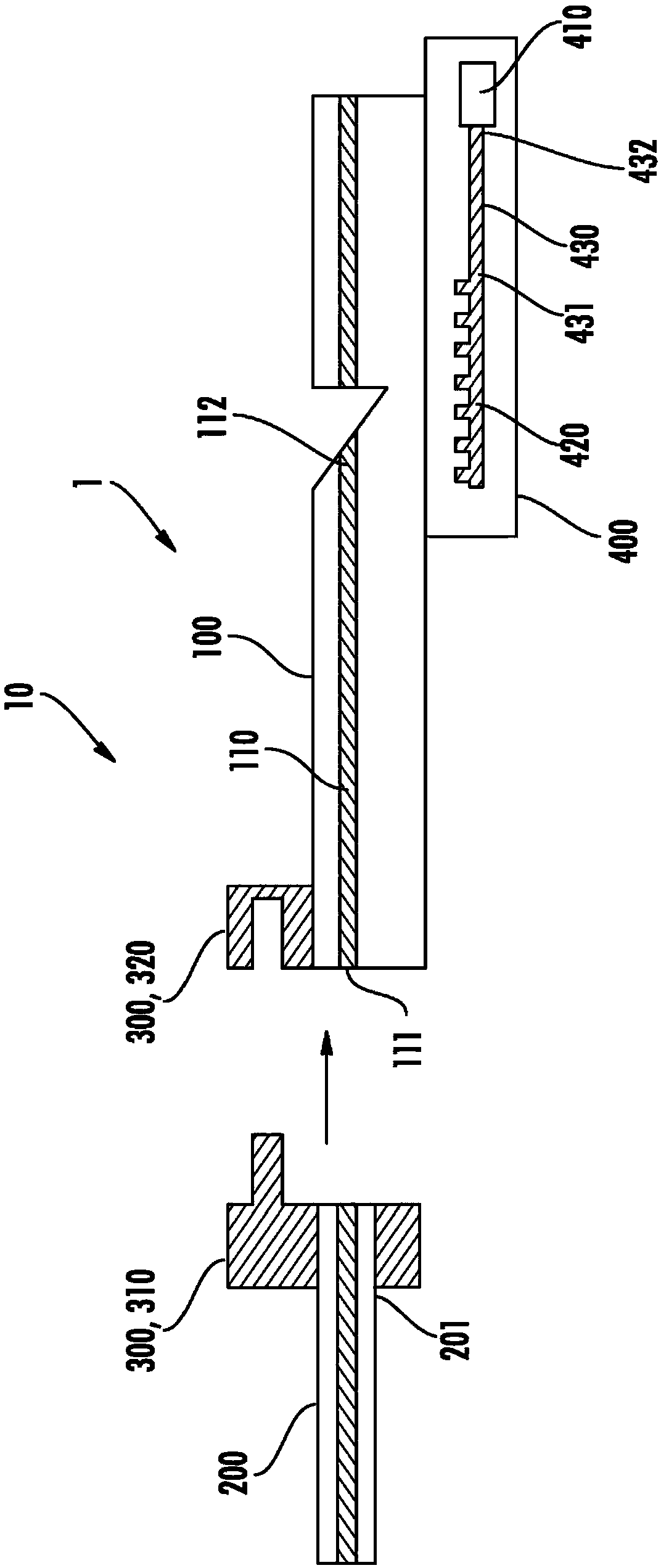
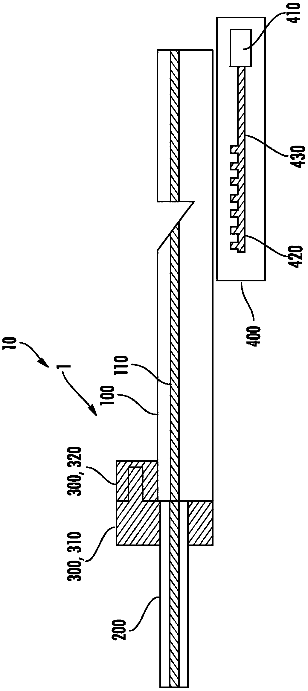
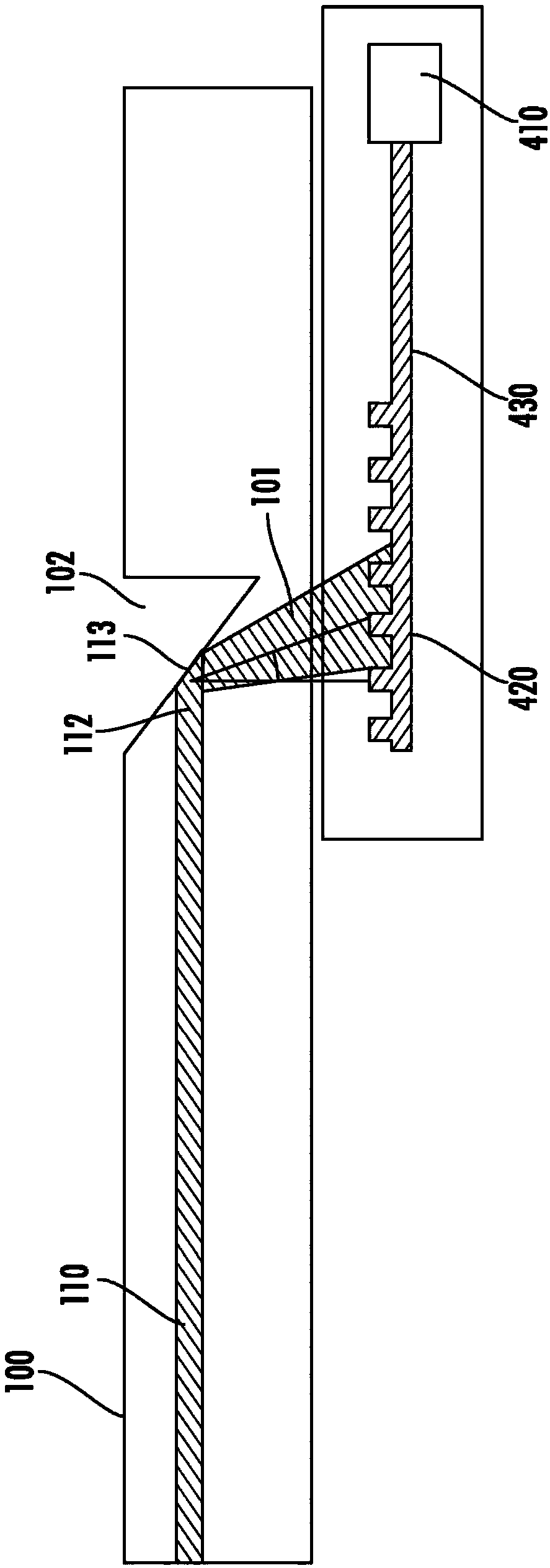
[0028] Figure 1A and 1B is shown in the unmated state ( Figure 1A ) and mating status ( Figure 1B) for coupling at least one optical fiber to at least one optoelectronic device. Arrangement 10 is disclosed in detail to convey the operation and concept of interposer assembly 1 . The interposer assembly 1 comprises an interposer 100 comprising at least one optical waveguide 110 having a first end 111 and a second end 112 optically coupled to at least one optical fiber 200 . The arrangement also includes a coupling device 300 for optically coupling the at least one optical fiber 200 to the interposer 100 and aligning the at least one optical fiber 200 to the at least one optical waveguide 110 so as to be between the at least one optical fiber 200 and the at least one optical waveguide 110 transmit light.
[0029] The coupling device 300 comprises a first part 310 arranged at the end 201 of the at least one optical fiber 200 and a second part 320 arranged at the edge of the ...
PUM
 Abstract
Description
Claims
Application Information
 - R&D
- Intellectual Property
- Life Sciences
- Materials
- Tech Scout
- Unparalleled Data Quality
- Higher Quality Content
- 60% Fewer Hallucinations
Browse by: Latest US Patents, China's latest patents, Technical Efficacy Thesaurus, Application Domain, Technology Topic, Popular Technical Reports.
© 2025 PatSnap. All rights reserved.Legal|Privacy policy|Modern Slavery Act Transparency Statement|Sitemap|About US| Contact US: help@patsnap.com