Semiconductor device and manufacturing method thereof
A manufacturing method and semiconductor technology, applied in semiconductor/solid-state device manufacturing, semiconductor devices, semiconductor/solid-state device components, etc., can solve problems such as splicing precision circuit disconnection, and achieve the effect of miniaturization, time and labor
- Summary
- Abstract
- Description
- Claims
- Application Information
AI Technical Summary
Problems solved by technology
Method used
Image
Examples
no. 1 approach
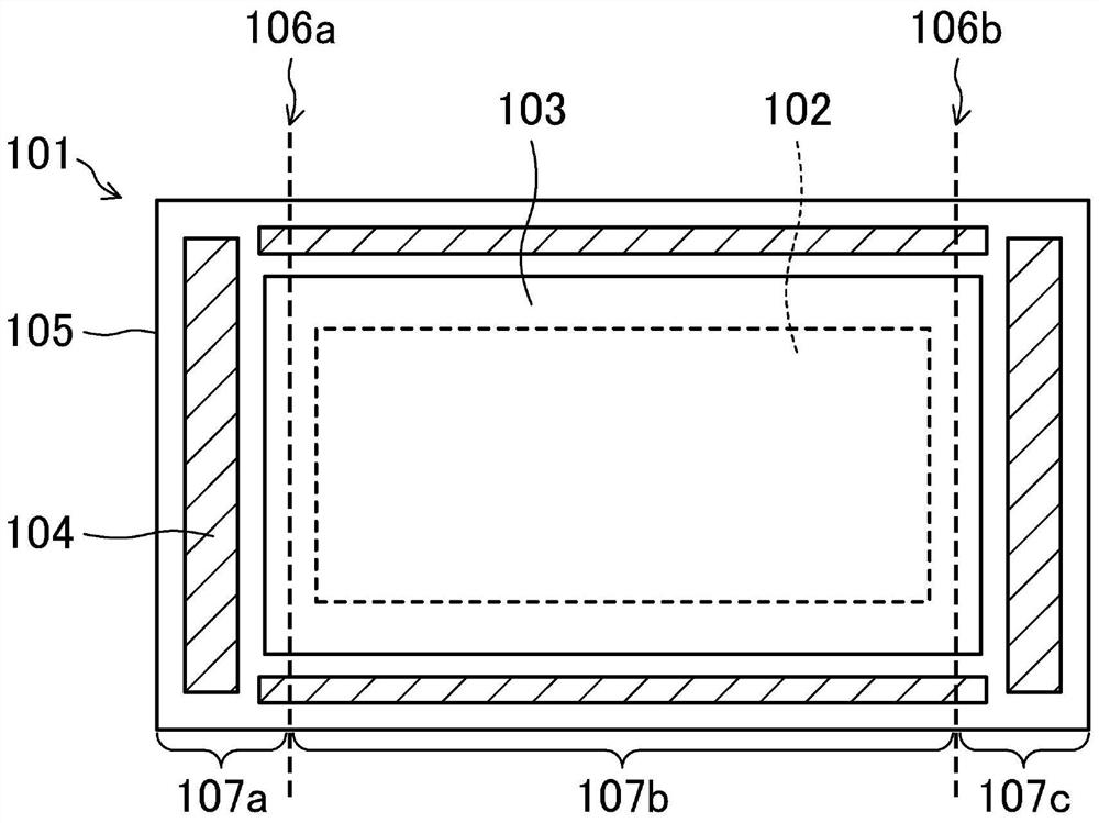
[0050] image 3 It is a schematic top view of the semiconductor device 101 exemplified in the present disclosure. The semiconductor device 101 is a solid-state imaging device, and has an imaging unit 102 located at a central position, and an imaging unit 103 including the imaging unit 102 therein. A peripheral circuit 104 is provided around the semiconductor device 101 , and a scribe region 105 is further located around the peripheral circuit 104 . Here, elements in the imaging unit 102 on the inner side are used when capturing moving images, and elements in the imaging unit 103 (both elements in the imaging unit 102 on the inner side and elements on the outside thereof) are used when capturing still images.
[0051] The pattern of the semiconductor device 101 is divided into a plurality of (here, three) patterns 107a, 107b, and 107c by the bonding parts 106a and 106b. These patterns are spliced by splicing exposure to manufacture the semiconductor device 101 .
[0052] I...
no. 2 approach
[0084] A second embodiment will be described. This embodiment also takes image 3 The illustrated semiconductor device 101 is described as an example.
[0085] exist Figure 10 In the figure, the first mask 201 for element formation and the mask 202 for second element formation used for splicing exposure for forming the element isolation layer of the semiconductor device 101 in this embodiment are shown.
[0086] Such as Figure 10 As shown, the first element forming mask 201 is a rectangle whose exposure region 203 has a height h and a width a, and has overlapping inspection marks 205a to 205h. In addition, the second element forming mask 202 is a rectangle whose exposure region 204 has a height h and a width b, and has overlapping inspection marks 206a to 206h.
[0087]These first and second element forming masks 201 and 202 have substantially the same structure as the first and second element forming masks 108 and 109 in the first embodiment, and include image 3 The p...
PUM
 Abstract
Description
Claims
Application Information


