Active matrix substrate, method for producing same, and display device

An active matrix and manufacturing method technology, applied in semiconductor/solid-state device manufacturing, optics, instruments, etc., can solve problems such as poor contact

Active Publication Date: 2018-12-21
SHARP KK
View PDF8 Cites 2 Cited by
  • Summary
  • Abstract
  • Description
  • Claims
  • Application Information

AI Technical Summary

Problems solved by technology

[0003] However, depending on the combination of the metal layer included in the metal wiring and the metal layer included in the connection wiring, there may be cases where contact failure occurs due to electrical corrosion.

Method used


Image

  • Active matrix substrate, method for producing same, and display device
  • Active matrix substrate, method for producing same, and display device
  • Active matrix substrate, method for producing same, and display device

Examples


no. 1 approach

[0073]

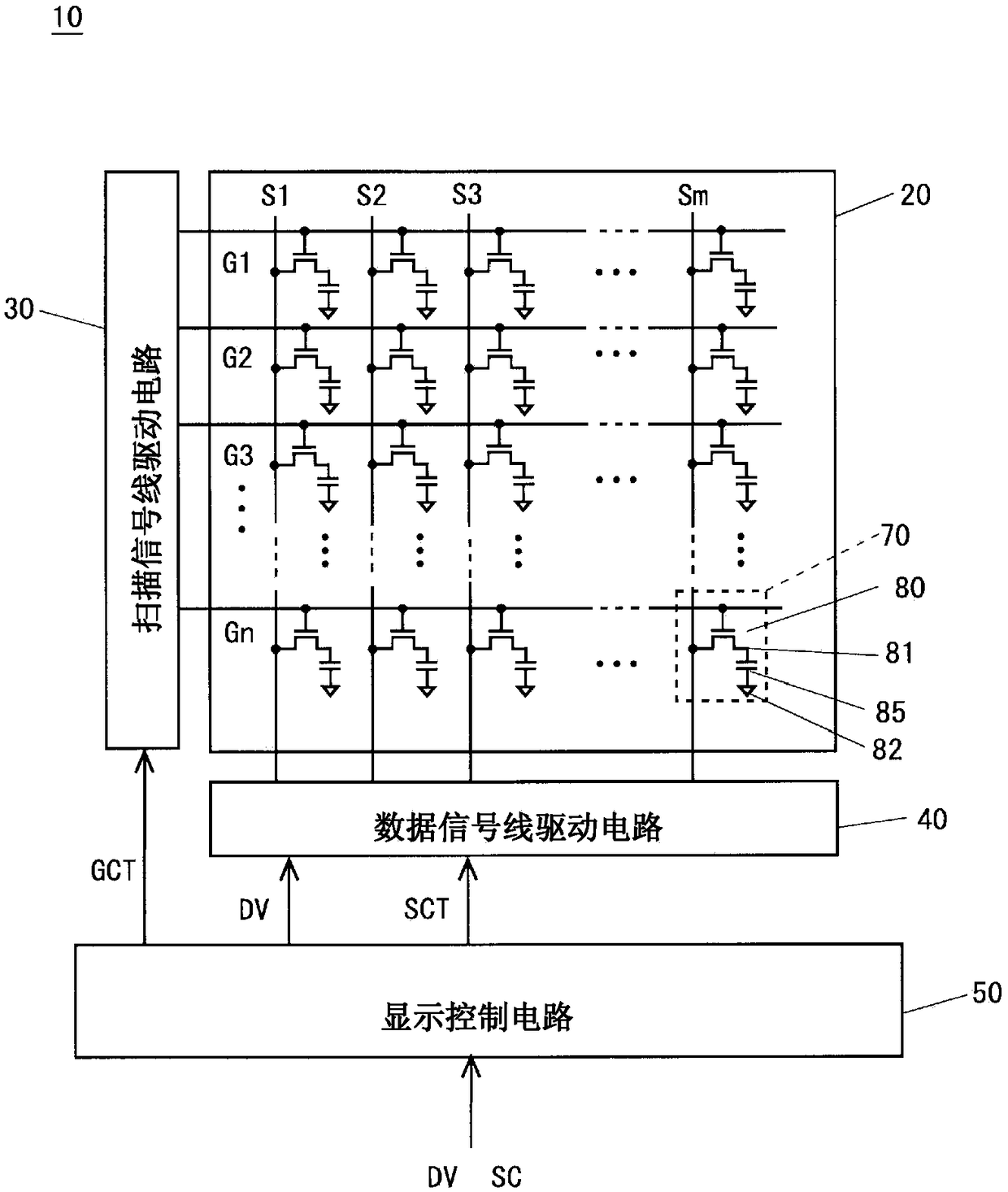
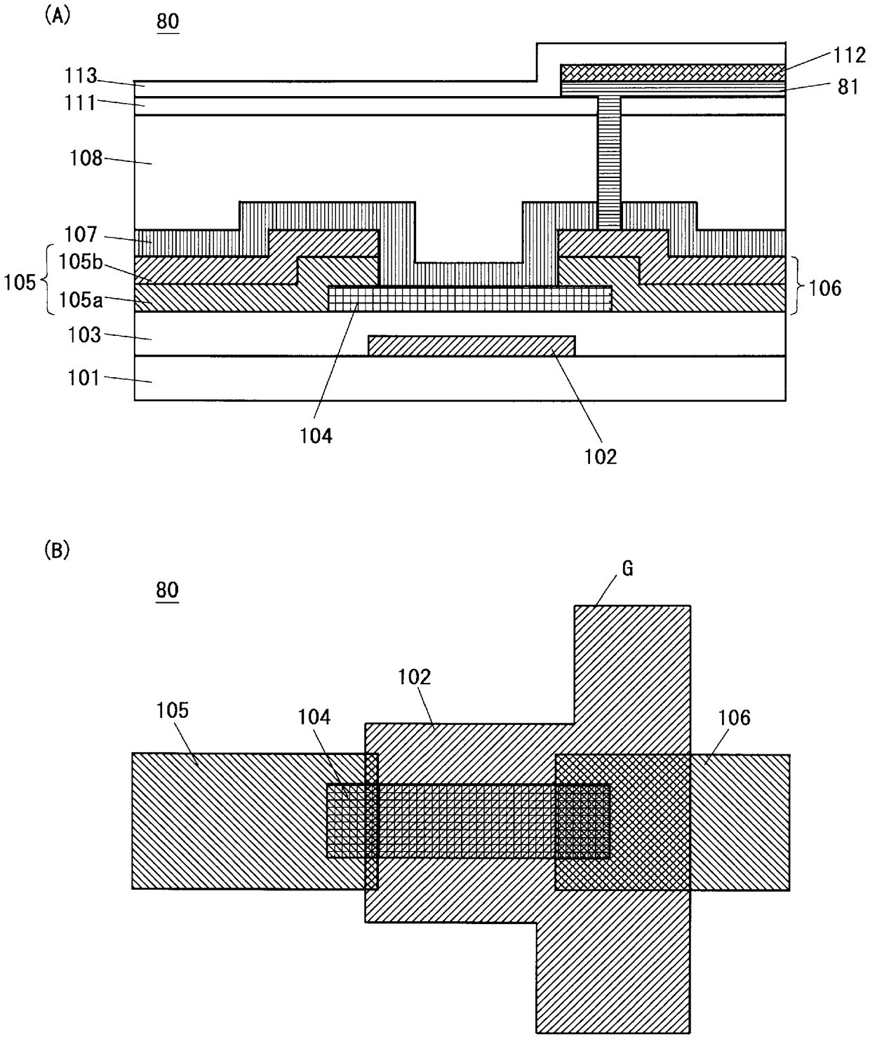
[0074] figure 1 It is a block diagram showing the configuration of a liquid crystal display device 10 including the active matrix substrate of the first embodiment. Such as figure 1 As shown, the liquid crystal display device 10 includes a liquid crystal panel 20, a scanning signal line driving circuit 30, a data signal line driving circuit 40, and a display control circuit 50. As will be described later, the liquid crystal panel 20 combines an active matrix substrate and a color filter The substrates are bonded together.

[0075] Formed on the liquid crystal panel 20 are: m data signal lines S1 to Sm; n scanning signal lines G1 to Gn; (m×n) pixel forming portions 70 . Each pixel forming portion 70 includes: a thin film transistor (Thin Film Transistor: TFT) 80, the gate electrode of which is connected to the scanning signal lines G1-Gn passing through the corresponding intersection, and the source electrode is connected to each data signal line passing through...

no. 2 approach

[0112]

[0113] Figure 8 is a diagram showing the structure of the wiring connection structure 151 included in the active matrix substrate 10a of the second embodiment, and more specifically, Figure 8 (A) is a sectional view showing the wiring connection structure 151, Figure 8 (B) is a plan view of the wiring connection structure 151 . Such as Figure 8 (A) and Figure 8 As shown in (B), the wiring connection structure 151 of this embodiment has the same Figure 4 The wiring connection configuration 150 shown is a very similar configuration. Therefore, yes Figure 8 (A) and Figure 8 In the wiring connection structure 151 shown in (B), the same structure as the wiring connection structure 150 is denoted by the same reference numeral, and the description is abbreviate|omitted, and a different structure is demonstrated.

[0114] and Figure 4 Similarly to the case shown, an opening 103 c is formed in the gate insulating film 103 inside the contact hole 140 . The e...

no. 3 approach

[0125]

[0126] Figure 10 is a diagram showing the structure of the wiring connection structure 152 included in the active matrix substrate 10a of the third embodiment, and more specifically, Figure 10 (A) is a sectional view of the wiring connection structure 152, Figure 10 (B) is a plan view of the wiring connection structure 152 . Such as Figure 10 (A) and Figure 10 As shown in (B), the wiring connection structure 152 of this embodiment has Figure 15 (A) and Figure 15 The conventional wiring connection structure 250 shown in (B) has a very similar structure. Therefore, yes Figure 10 (A) and Figure 10 In the wiring connection structure 152 shown in (B), the same structure as the wiring connection structure 250 is denoted by the same reference numeral, and description is abbreviate|omitted, and a different structure is demonstrated.

[0127] Such as Figure 10 (A) and Figure 10 As shown in (B), in the wiring connection structure 152 of this embodiment, the...


PUM

PropertyMeasurementUnit
thicknessaaaaaaaaaa

Abstract

Provided are: an active matrix substrate having a highly reliable wiring connection structure; a method for producing same; and a display device. A first metal wiring 122 and a second metal wiring 125are electrically connected via an IGZO layer 124 which has been made conductive. When the connection is formed, the second metal wiring 125 and an ITO layer 109 are separated and not being in contactwith each other since a passivation layer 107 and an organic insulating film 108 are formed between the second metal wiring 125 and the ITO layer 109. This configuration prevents contact failure dueto electric corrosion occurring between the ITO layer 109 and an aluminum layer 125a of the second metal wiring 125, and thus enables providing of a highly reliable wiring connection structure.

Description

technical field [0001] The present invention relates to an active matrix substrate, its manufacturing method and a display device, and particularly relates to an active matrix substrate capable of preventing poor contact caused by electric corrosion, its manufacturing method and a display device. Background technique [0002] When a plurality of metal wirings are formed from the metal film of the same layer, they may intersect. In this case, by substituting one of the two intersecting metal wirings with a metal wiring formed of a metal film of another layer, it is possible to avoid crossing of the metal wirings. In order to switch metal wiring made of one layer to metal wiring made of another layer in this way, it is necessary to pass the metal wiring made of a metal film of one layer and the metal wiring made of a metal film of another layer through Connection wires made of metal films of layers different from these are connected. [0003] However, depending on the combin...

Claims


Application Information

Patent Timeline
Patent Type & Authority Applications(China)
IPC IPC(8): H01L21/768G02F1/1345G02F1/1368H01L23/522H01L29/786
CPCG02F1/136227G02F1/136286H01L27/1225H01L27/124G02F1/136295H01L21/768H01L23/522H01L29/786G02F1/1368G02F1/133345
Inventor 冈部达锦博彦家根田刚士
Owner SHARP KK
Why Eureka
Try Eureka