A method for smoothing the surface of copper-catalyzed etching textured silicon wafers

A silicon chip surface, copper catalysis technology, applied in the direction of final product manufacturing, sustainable manufacturing/processing, semiconductor/solid-state device manufacturing, etc., can solve the problems of reduced efficiency of battery components, excessive series resistance, and low minority carrier lifetime. Achieve the effects of solving poor passivation, improving minority carrier life, and improving battery efficiency

Active Publication Date: 2020-07-31
KUNMING UNIV OF SCI & TECH
View PDF8 Cites 1 Cited by
  • Summary
  • Abstract
  • Description
  • Claims
  • Application Information

AI Technical Summary

Problems solved by technology

[0004] The present invention aims at the problem that the surface of the diamond wire-cut silicon wafer is processed by MCCE method and the sharp structure existing on the inverted pyramid is introduced into the surface, which makes it difficult to effectively cover the anti-reflection film, the minority carrier life is too low, and the series resistance is too large, which leads to the decrease of the efficiency of the battery module. The problem is to provide a method for smoothing the surface of silicon wafers made of copper-catalyzed etching, that is, using a low-cost metal copper-catalyzed chemical etching method to realize the controllable preparation of large-scale inverted pyramid arrays on the silicon-based surface, and obtain Smooth inverted pyramid structure textured silicon wafer; the micro-surface structure of the silicon wafer is smooth and has no sharp structure, which can remove the recombination center, improve the minority carrier lifetime, solve the problems of poor passivation, and effectively improve the efficiency of the battery

Method used


Image

  • A method for smoothing the surface of copper-catalyzed etching textured silicon wafers
  • A method for smoothing the surface of copper-catalyzed etching textured silicon wafers
  • A method for smoothing the surface of copper-catalyzed etching textured silicon wafers

Examples


Embodiment 1

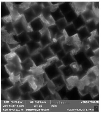
[0032] Embodiment 1: a kind of method for the surface smooth treatment of copper catalyzed etching textured silicon wafer, concrete steps are:

[0033] (1) Carry out cleaning and oxide layer removal treatment to the silicon chip cut by diamond wire; wherein the silicon chip is a polycrystalline silicon chip, the average thickness of the amorphous silicon layer covered by the surface layer of the silicon chip cut by diamond wire is 50nm, and the line marks on the surface of the silicon chip are average The height is 4 μm; the cleaning method is to place the diamond wire-cut silicon wafer in acetone, ethanol and deionized water for 10 minutes; The mass percentage concentration is 10%;

[0034] (2) Introduction of an inverted pyramid structure: at room temperature, place the silicon wafer after the oxide layer removal treatment in step (1) in HF-Cu(NO 3 ) 2 -H 2 o 2 Etched in the etching solution for 3min, in which HF-Cu(NO 3 ) 2 -H 2 o 2 The concentration of HF in the et...

Embodiment 2

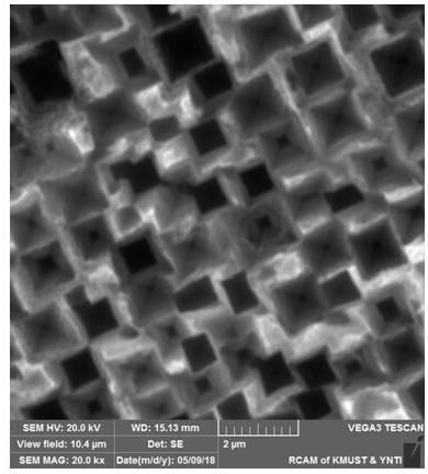
[0038] Embodiment 2: a kind of method for the surface smooth treatment of copper catalyzed etching textured silicon chip, concrete steps are:

[0039] (1) Carry out cleaning and oxidation layer removal processing to the silicon chip of diamond wire cutting; Wherein silicon chip is monocrystalline silicon chip, the average thickness of the amorphous silicon layer covered by the silicon chip surface layer of diamond wire cutting is 30nm, the silicon chip surface The average height of the line marks is 4 μm; the cleaning method is to place the diamond wire-cut silicon wafer in acetone, ethanol and deionized water for 10 minutes; the method of oxide layer removal treatment is to soak the silicon wafer in HF solution for 30 minutes Wherein the mass percentage concentration of HF solution is 10%;

[0040] (2) Introduction of an inverted pyramid structure: at a temperature of 30°C, place the silicon wafer after the oxidation layer removal treatment in step (1) in HF-CuSO 4 -H 2 o ...

Embodiment 3

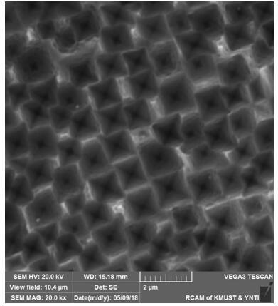
[0043] Embodiment 3: a kind of method for the surface smooth treatment of copper catalyzed etching textured silicon chip, concrete steps are:

[0044] (1) Carry out cleaning and oxide layer removal treatment to the silicon chip cut by diamond wire; wherein the silicon chip is a polycrystalline silicon chip, the average thickness of the amorphous silicon layer covered by the surface layer of the silicon chip cut by diamond wire is 50nm, and the line marks on the surface of the silicon chip are average The height is 4 μm; the cleaning method is to place the diamond wire-cut silicon wafer in acetone, ethanol and deionized water for 10 minutes; The mass percentage concentration is 10%;

[0045] (2) Introduction of an inverted pyramid structure: at a temperature of 60°C, place the silicon wafer after the oxide layer removal treatment in step (1) in HF-CuBr 2 -H 2 o 2 Etching in etching solution for 6min, in which HF-CuBr 2 -H 2 o 2 The concentration of HF in the etching solut...


PUM

PropertyMeasurementUnit
thicknessaaaaaaaaaa
heightaaaaaaaaaa
thicknessaaaaaaaaaa

Abstract

The invention relates to a method for smoothly treating the surface of a copper-catalyzed etching velvet-making silicon wafer, belonging to the technical field of surface velvet-making of crystallinesilicon in the solar cell industry. The invention cleans the silicon wafer of the diamond wire cutting and removes the oxide layer. At room temperature ~ 95 degree centigrade, that silicon wafer afterthe oxide lay removal treatment is placed in HF-Metal copper salt-H2O2 etch solution is etched for 1-600 min, then immerse in nitric acid solution for 1-100 min, then immersed in HF solution for 1-100 min, and then cleaned with deionized water to obtain inverted pyramid textured silicon wafer; A smooth invert pyramid structure woven silicon wafer is obtained by smoothing the inverted pyramid structure woven silicon wafer; The method of smoothing treatment is to adopt smoothing treatment system method and / or ultrasonic treatment method. The method of the invention can realize the inverted pyramid smooth pile-making structure obtained by the low-cost MCCE method.

Description

technical field [0001] The invention relates to a method for smoothing the surface of a silicon chip made of texture by copper-catalyzed etching, and belongs to the technical field of texture of the surface of crystalline silicon in the solar cell industry. Background technique [0002] At present, with the widespread promotion of diamond wire slicing technology, and in view of the failure of the traditional mortar cutting method to use acid texturing on diamond wire cut polysilicon wafers, it is urgent to find a feasible and low-cost texturing method. Metal Catalyzed Etching Texturing (MCCE) is expected to break through the challenges of efficient texturing on the surface of diamond wire-cut silicon wafers, and has attracted much attention. In view of the high cost of using noble metals (Ag, Au, Pt, etc.) Not only does it have a good effect of removing line marks, but also obtains an excellent light trapping effect. At the same time, it has the advantages of lower cost and...

Claims


Application Information

Patent Timeline
Patent Type & Authority Patents(China)
IPC IPC(8): H01L21/306H01L31/18H01L31/0236
CPCH01L21/30604H01L31/02363H01L31/1804Y02E10/547Y02P70/50
Inventor 李绍元盛贵章马文会朱祺桉陈正杰万小涵于洁魏奎先雷云颜恒维杨斌戴永年
Owner KUNMING UNIV OF SCI & TECH
Why Eureka
Try Eureka