
Data latch circuit, page data latch and method for flash memory page programming

A data latch and flash page technology, applied in the data latch circuit of flash page programming and the field of page data latch, can solve the problems of large size and small driving ability, and achieve the reduction of product cost, area reduction, and improvement of competition. force effect

Active Publication Date: 2020-12-01
PUYA SEMICON SHANGHAI CO LTD
View PDF6 Cites 0 Cited by
  • Summary
  • Abstract
  • Description
  • Claims
  • Application Information

AI Technical Summary

Problems solved by technology

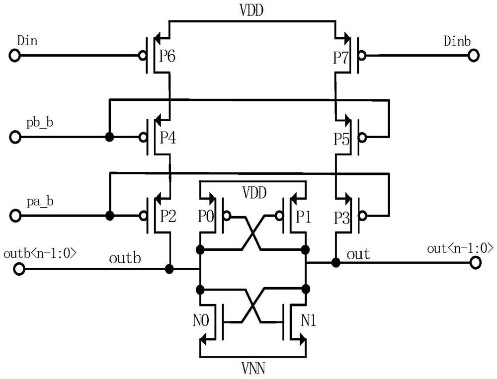
Since P2, P4, and P6 are connected in series, the drive capacity is small, so a larger size is required

Method used


Image

  • Data latch circuit, page data latch and method for flash memory page programming
  • Data latch circuit, page data latch and method for flash memory page programming
  • Data latch circuit, page data latch and method for flash memory page programming

Examples


Embodiment Construction

[0039] The present invention will be further elaborated below by describing a preferred specific embodiment in detail in conjunction with the accompanying drawings.

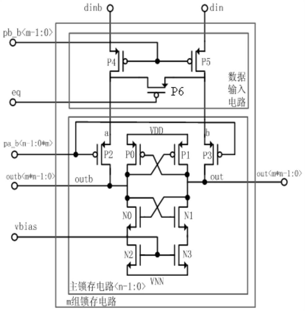
[0040] Such as figure 2 As shown, the present invention is a kind of data latch circuit that is used for flash memory page programming, comprises: data input circuit, n groups of master latch circuits that are connected with described data input circuit; Each group of master latch circuits includes: the first transistor P0, the second transistor P1, the third transistor P2, the fourth transistor P3, the eighth transistor N0, the ninth transistor N1, the tenth transistor N2 and the eleventh transistor N3.

[0041] The sources of the first transistor P0 and the second transistor P1 are connected in series as the input terminal of the power supply VDD.

[0042] The drain of the first transistor P0 is connected to the gate (gate) of the second transistor P1 in reverse, and the drain of the second transisto...


PUM


Abstract

The invention discloses a data latch circuit for flash memory page programming, a page data latch and a method thereof. The data latch circuit comprises a data input circuit and n groups of main latchcircuits connected with the data input circuit. The data input circuit includes a fifth transistor, a sixth transistor and a seventh transistor. The gate of the fifth transistor and the gate of the sixth transistor are inversely connected in series with the input pb_b signal. The source of the sixth transistor serves as an input terminal of the data Din; the source of the fifth transistor servesas an input terminal of the inverting data Dinb of the data Din; the gate of the seventh transistor inputs an inverted eq signal for balancing the drain voltages of the fifth transistor and the sixthtransistor to prevent crosstalk during data writing; the drains of the fifth transistor and the seventh transistor are connected to the inputs a of each main latch circuit. The drain of the sixth transistor and the source of the seventh transistor are connected to the inputs b of the respective main latch circuits. The invention has the advantages of increasing driving capacity and saving circuitarea.

Description

technical field [0001] The invention relates to the field of memory, in particular to a data latch circuit for flash page programming, a page data latch and a method. Background technique [0002] In the flash memory based on the SONOS process, each bit line needs to correspond to a set of data latches, and the data in all the latches are simultaneously written into the memory array during page programming. In the flash memory, a large number of data latches are required, while traditional data latches have a large number of devices, a large size, and a large circuit area. A flash memory generally includes 1024 page data latches of the main latch circuit, or even more. [0003] Conventional data latches such as figure 1 As shown, the data Din and Dinb (Dinb is the inverse of Din) are added to the gates of P6 and P7. pa_b and pb_b select data latches through P2, P3, P4, and P5 respectively. Since P2, P4, and P6 are connected in series, the drive capacity is small, so a la...

Claims


Application Information

Patent Timeline
Patent Type & Authority Patents(China)
IPC IPC(8): G11C16/10
CPCG11C16/10
Inventor 冯国友李兆桂
Owner PUYA SEMICON SHANGHAI CO LTD
Learn More