Liquid Crystal Display Device and Electronic Device Including the Same

a liquid crystal display and electronic device technology, applied in semiconductor devices, digital storage, instruments, etc., can solve the problems of image not being displayed, hard to operate the driver circuit, etc., to achieve the effect of increasing the potency of the transistor, preventing malfunction, and increasing the vgs of the transistor

Active Publication Date: 2010-07-22
SEMICON ENERGY LAB CO LTD
View PDF20 Cites 40 Cited by
  • Summary
  • Abstract
  • Description
  • Claims
  • Application Information

AI Technical Summary

Benefits of technology

[0048]According to one embodiment of the present invention, the potential of a transistor can be increased. Alternatively, according to one embodiment of the present invention, malfunction can be prevented. Alternatively, according to one embodiment of the present invention, Vgs of a transistor can be increased. Alternatively, according to one embodiment of the present invention, the on-resistance of a transistor can be made low. Alternatively, according to one embodiment of the present invention, the channel width of a transistor can be reduced. Alternatively, according to one embodiment of the present invention, the deterioration of a transistor can be suppressed or eased. Alternatively, according to one embodiment of the present invention, a layout area can be reduced. Alternatively, according to one embodiment of the present invention, a falling time or a rising time of an output signal of a flip-flop, a shift register, or a driver circuit such as a scan line driver circuit can be shortened. Alternatively, according to one embodiment of the present invention, the size of a display device can be increased. Alternatively, according to one embodiment of the present invention, a high-definition display device can be obtained. Alternatively, according to one embodiment of the present invention, a frame of a display device can be narrowed. Alternatively, according to one embodiment of the present invention, a correct signal can be written to a pixel. Alternatively, according to one embodiment of the present invention, display quality can be improved. Alternatively, according to one embodiment of the present invention, yield can be increased. Alternatively, according to one embodiment of the present invention, cost can be reduced. Alternatively, according to one embodiment of the present invention, distortion or delay of a signal to be input to a shift register can be reduced. Alternatively, according to one embodiment of the present invention, power consumption can be reduced. Alternatively, according to one embodiment of the present invention, the current capability of an external circuit can be reduced. Alternatively, according to one embodiment of the present invention, the size of an external circuit or the size of a display device including the external circuit can be reduced.

Problems solved by technology

As the deterioration of the transistor advances, there is a problem in that the driver circuit becomes hard to operate and an image cannot be displayed.

Method used


Image

  • Liquid Crystal Display Device and Electronic Device Including the Same
  • Liquid Crystal Display Device and Electronic Device Including the Same
  • Liquid Crystal Display Device and Electronic Device Including the Same

Examples


embodiment 1

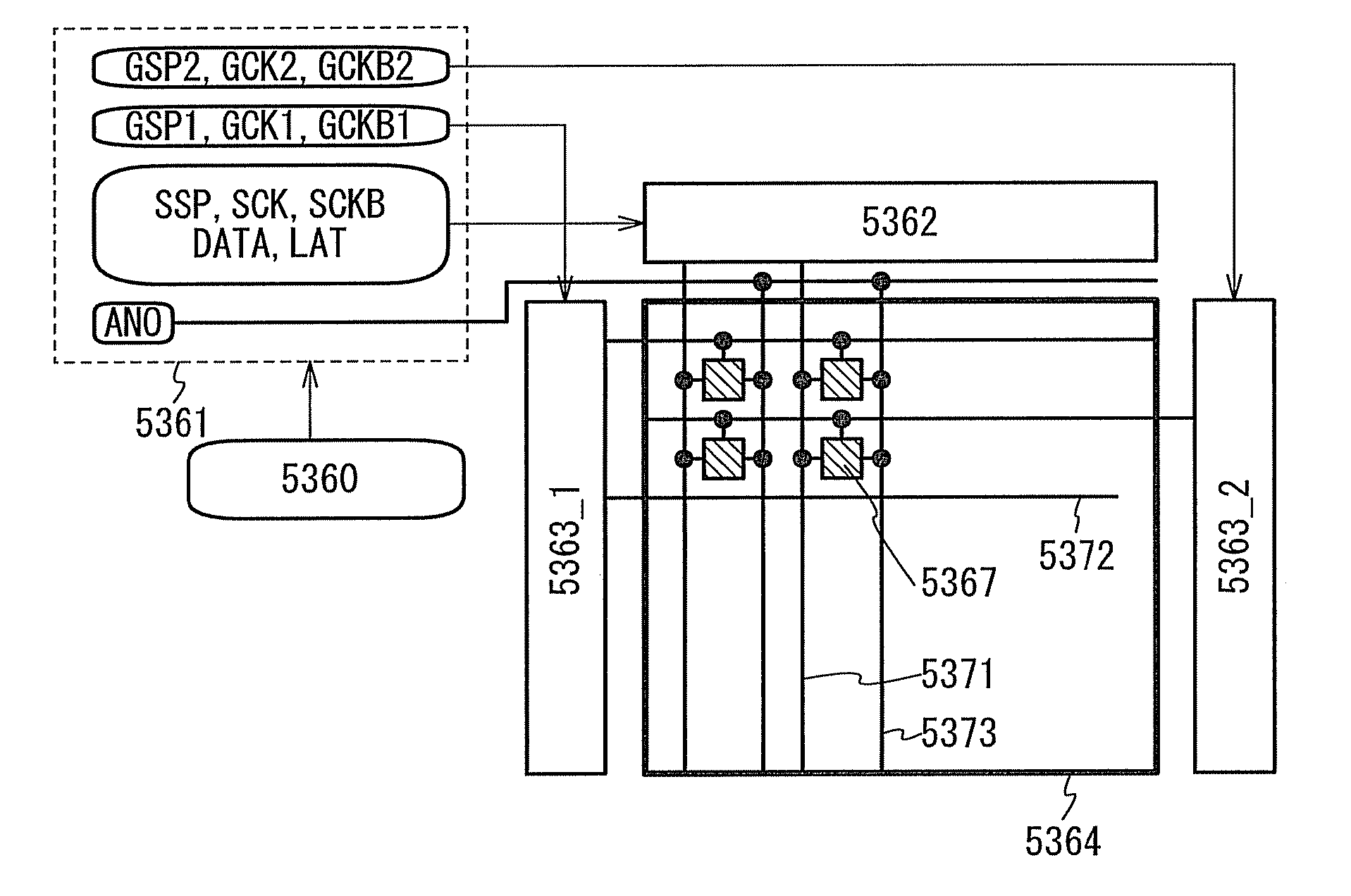
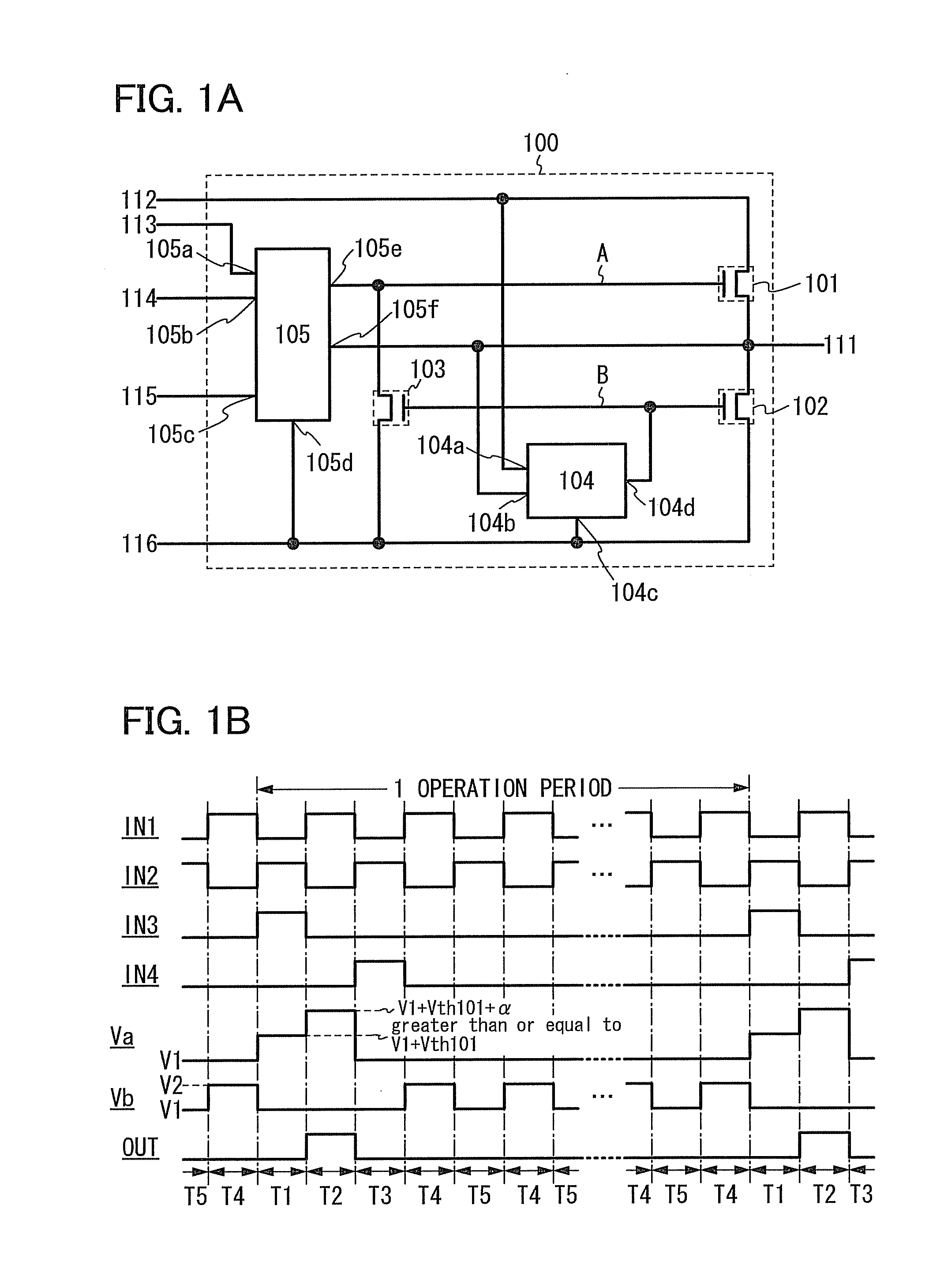
[0087]In this embodiment, an example of a semiconductor device is described. The semiconductor device in this embodiment can be used for a shift register, a gate driver, a source driver, a display device, or the like, for example. Note that the semiconductor device can be referred to as a flip-flop or a driver circuit.

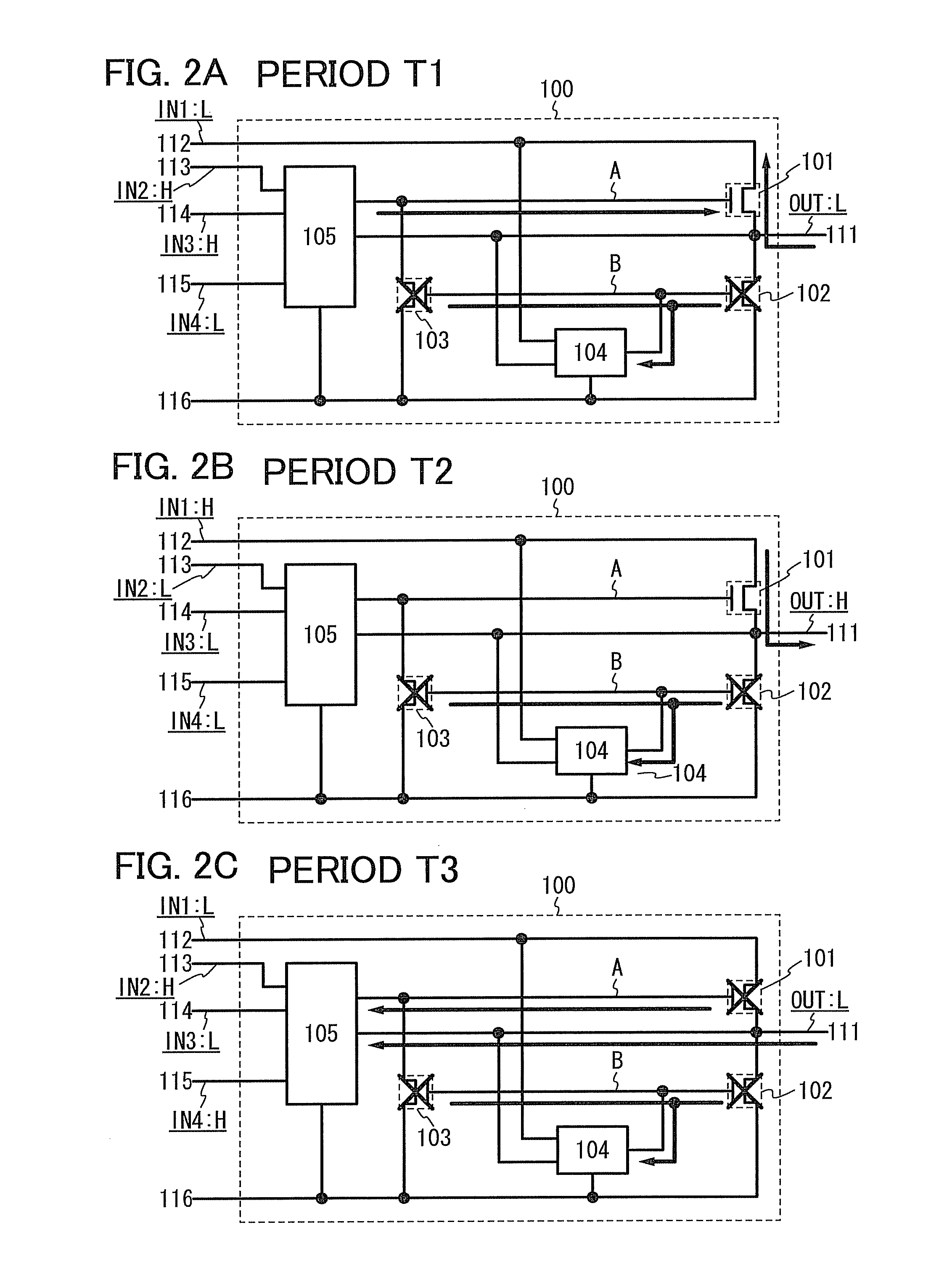
[0088]First, an example of the semiconductor device in this embodiment is described with reference to FIG. 1A. A circuit 100 is shown in FIG. 1A. Note that the circuit 100 can be referred to as a semiconductor device, a driver circuit, or a flip-flop.

[0089]The circuit 100 includes a transistor 101 (also referred to as a first transistor), a transistor 102 (also referred to as a second transistor), a transistor 103 (also referred to as a third transistor), a circuit 104 (also referred to as a first circuit), and a circuit 105 (also referred to as a second circuit). The circuit 104 includes a plurality of terminals: a terminal 104a, a terminal 104b, a terminal 104c, and ...

embodiment 2

[0157]In this embodiment, a specific example of the circuit 104 described in Embodiment 1 is described. Note that the circuit 104 can be referred to as a semiconductor device, a driver circuit, or a gate driver. Note that description of the content described in Embodiment 1 is omitted. Note that the content described in Embodiment 1 can be freely combined with a content described in this embodiment.

[0158]First, one example of the circuit 104 is described with reference to FIG. 9A. In the example in FIG. 9A, the circuit 104 includes a transistor 201 (also referred to as a fourth transistor), a transistor 202 (also referred to as a fifth transistor), a transistor 203 (also referred to as a sixth transistor), and a transistor 204 (also referred to as a seventh transistor). However, this embodiment is not limited to this example. Any of these transistors can be eliminated. Alternatively, any of these transistors can be replaced with any of a variety of elements such as a capacitor, a re...

embodiment 3

[0194]In this embodiment, a specific example of the circuit 105 is described. Note that the circuit 105 can be referred to as a semiconductor device, a driver circuit, or a gate driver. Note that description of the content described in Embodiment 1 or 2 is omitted. Note that the content described in Embodiment 1 or 2 can be freely combined with a content described in this embodiment.

[0195]First, one example of the circuit 105 is described with reference to FIG. 12A. In the example in FIG. 9A, the circuit 105 includes a transistor 301 (also referred to as an eighth transistor), a transistor 302 (also referred to as a ninth transistor), a transistor 303 (also referred to as a tenth transistor), a transistor 304 (also referred to as an eleventh transistor), and a transistor 305 (also referred to as a twelfth transistor). However, this embodiment is not limited to this example. Any of these transistors can be eliminated. Alternatively, any of these transistors can be replaced with any o...


PUM

PropertyMeasurementUnit
threshold voltageaaaaaaaaaa
currentsaaaaaaaaaa
currentsaaaaaaaaaa

Abstract

A driver circuit includes first to third transistors, a first circuit, and a second circuit. In the first transistor, a first terminal is electrically connected to a second wiring, a second terminal is electrically connected to a first wiring, and a gate is electrically connected to the second circuit and a first terminal of the third transistor. In the second transistor, a first terminal is electrically connected to the first wiring, a second terminal is electrically connected to a sixth wiring, a gate is electrically connected to the first circuit and a gate of the third transistor. A second terminal of the third transistor is electrically connected to the sixth wiring. The first circuit is electrically connected to a third wiring, a fourth wiring, a fifth wiring, and the sixth wiring. The second circuit is electrically connected to the first wiring, the second wiring, and the sixth wiring.

Description

BACKGROUND OF THE INVENTION[0001]1. Field of the Invention[0002]The present invention relates to a semiconductor device, a display device, a liquid crystal display device, a driving method thereof, or a producing method thereof. Specifically, the present invention relates to a semiconductor device, a display device, or a liquid crystal display device including a driver circuit formed over the same substrate as a pixel portion, or a driving method of the devices. Alternatively, the present invention relates to an electronic device including the semiconductor device, the display device, or the liquid crystal display device.[0003]2. Description of the Related Art[0004]In recent years, with the increase of large display devices such as liquid crystal televisions, display devices have been actively developed. Specifically, a technique of forming a driver circuit such as a gate driver over the same substrate as a pixel portion by using a transistor formed using a non-single-crystal semico...

Claims


Application Information

Patent Timeline
Patent Type & Authority Applications(United States)
IPC IPC(8): G09G3/36G02F1/1368
CPCG02F1/13454H01L23/528G02F2001/13606G02F2201/124H01L27/1214H01L29/786H01L29/7869G09G3/3677G09G3/3688G09G2300/0408G09G2300/0417G09G2310/0286G11C19/28H01L2924/0002G02F1/136286H01L2924/00G02F1/13606G09G3/3648G09G2320/043G09G2230/00G09G3/3674
Inventor UMEZAKI, ATSUSHI
Owner SEMICON ENERGY LAB CO LTD
Why Eureka
Try Eureka