An epitaxial structure of a deep ultraviolet LED chip and a preparation method thereof

A technology of LED chip and epitaxial structure, which is applied in the direction of semiconductor devices, electrical components, circuits, etc., can solve the problems of quantum well active area loss, disadvantage, and improve the light output of deep ultraviolet LED, so as to improve the light extraction efficiency and light output power. , The effect of improving extraction efficiency

Inactive Publication Date: 2018-12-28
EZHOU INST OF IND TECH HUAZHONG UNIV OF SCI & TECH +1
View PDF3 Cites 1 Cited by
  • Summary
  • Abstract
  • Description
  • Claims
  • Application Information

AI Technical Summary

Problems solved by technology

However, the low light extraction efficiency of deep ultraviolet LEDs still cannot meet the current application requirements. As mentioned above, in the prior art, in order to etch and leak the N-type contact layer, the N-type contact layer usually has a vertical bending angle α (as shown in the attached Figure 4 And attached Figure 5 ), the light emitted by the quantum well of deep ultraviolet LED is mainly in TM mode, and the light of TM mode is more emitted from the side wall of quantum well, which cannot be collected after flip-chip packaging, which is not conducive to improving the light output of deep ultraviolet LED; currently The commonly used device technology does not pay too much attention to the mesa etching of the deep ultraviolet LED, and the side wall of the active region of this design will cause the loss of the active region of the quantum well, which is not conducive to improving the light output of the deep ultraviolet LED.
[0004] Based on the epitaxial structure of the conventional deep ultraviolet LED chip, the loss of the active region of the quantum well will be caused, which is not conducive to improving the light output of the deep ultraviolet LED. It is urgent to develop a deep ultraviolet LED that can effectively improve the extraction efficiency of the side wall deep ultraviolet light. Chip epitaxial structure

Method used


Image

  • An epitaxial structure of a deep ultraviolet LED chip and a preparation method thereof
  • An epitaxial structure of a deep ultraviolet LED chip and a preparation method thereof
  • An epitaxial structure of a deep ultraviolet LED chip and a preparation method thereof

Examples


Embodiment 1

[0038] 1. Epitaxial structure of a deep ultraviolet LED chip

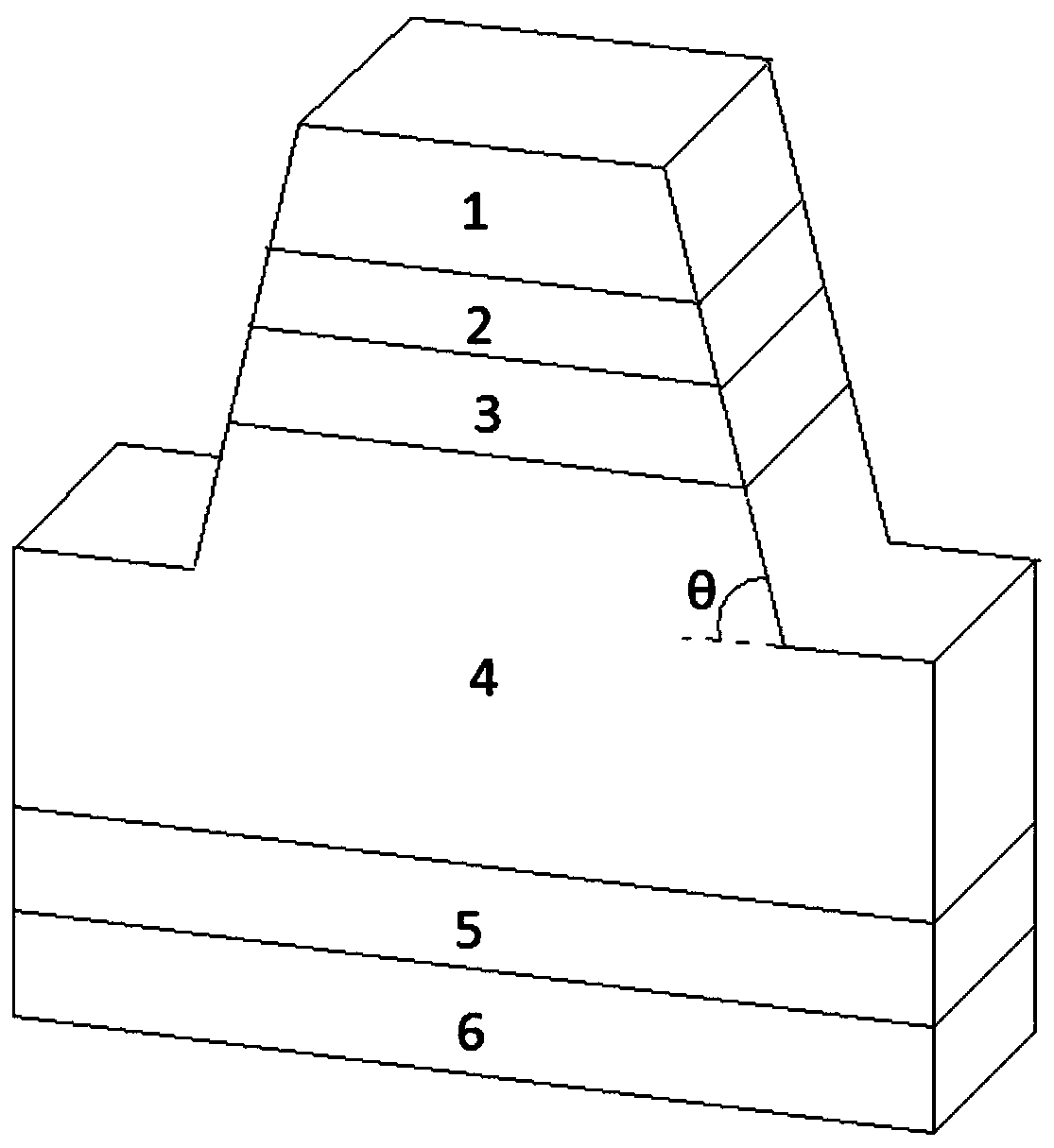
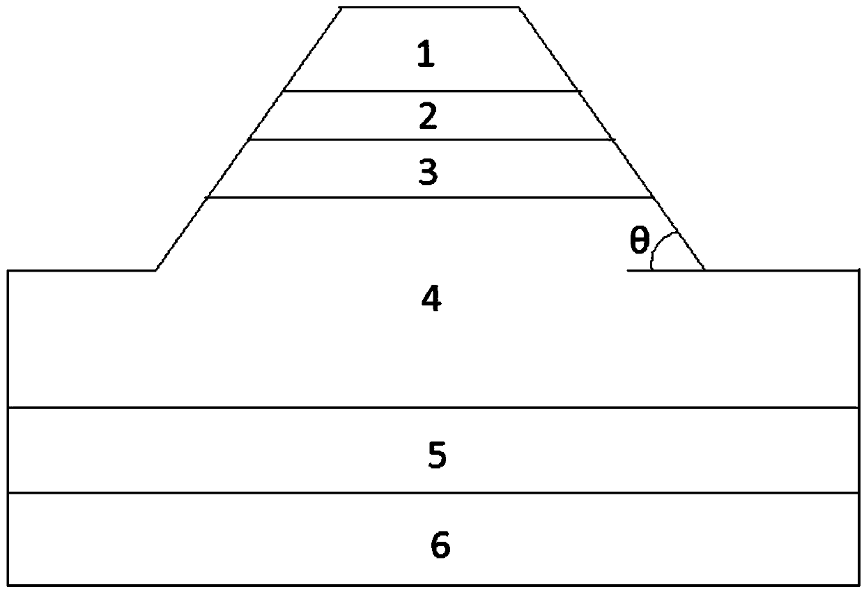
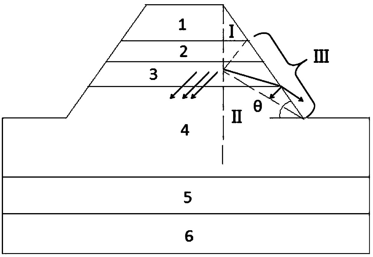
[0039] Such as Figure 1-3 As shown, an epitaxial structure of a deep ultraviolet LED chip, including a P-type GaN layer 1, a P-type AlGaN layer 2, a multi-quantum well active layer 3, an N-type AlGaN layer 4, an AlN layer 5 and a sapphire substrate connected in sequence 6. The multi-quantum well active layer 3 and the N-type AlGaN layer 4 jointly form an adjustment layer, and the adjustment layer has at least one inclined side, and the sandwich between the inclined side and the horizontal section near the center side of the adjustment layer The angle is the included angle of mesa etching, and the included angle of mesa etching is 28 degrees.

[0040]The adjustment layer has a plurality of inclined sides, and the mesa etching angles corresponding to the plurality of inclined sides are all 28 degrees.

[0041] The sloped sides include a first sloped side disposed on the multi-quantum well active layer 3 and a seco...

Embodiment 2

[0054] 1. Epitaxial structure of a deep ultraviolet LED chip

[0055] Such as Figure 1-3 As shown, an epitaxial structure of a deep ultraviolet LED chip, including a P-type GaN layer 1, a P-type AlGaN layer 2, a multi-quantum well active layer 3, an N-type AlGaN layer 4, an AlN layer 5 and a sapphire substrate connected in sequence 6. The multi-quantum well active layer 3 and the N-type AlGaN layer 4 jointly form an adjustment layer, and the adjustment layer has at least one inclined side, and the sandwich between the inclined side and the horizontal section near the center side of the adjustment layer The angle is the included angle of mesa etching, and the included angle of mesa etching is 35 degrees.

[0056] The adjustment layer has a plurality of inclined sides, and the mesa etching angles corresponding to the plurality of inclined sides are all 35 degrees.

[0057] The sloped sides include a first sloped side disposed on the multi-quantum well active layer 3 and a sec...

Embodiment 3

[0070] 1. Epitaxial structure of a deep ultraviolet LED chip

[0071] Such as Figure 1-3 As shown, an epitaxial structure of a deep ultraviolet LED chip, including a P-type GaN layer 1, a P-type AlGaN layer 2, a multi-quantum well active layer 3, an N-type AlGaN layer 4, an AlN layer 5 and a sapphire substrate connected in sequence 6. The multi-quantum well active layer 3 and the N-type AlGaN layer 4 jointly form an adjustment layer, and the adjustment layer has at least one inclined side, and the sandwich between the inclined side and the horizontal section near the center side of the adjustment layer The angle is the included angle of mesa etching, and the included angle of mesa etching is 40 degrees.

[0072] The adjustment layer has a plurality of inclined sides, and the mesa etching angles corresponding to the plurality of inclined sides are all 40 degrees.

[0073] The sloped sides include a first sloped side disposed on the multi-quantum well active layer 3 and a sec...


PUM


Abstract

The invention provides an epitaxial structure of a deep ultraviolet LED chip, which includes a P-type GaN layer, a P-type AlGaN layer, a multiple quantum well active layer, an N-type AlGaN layer, an AlN layer and a sapphire substrate which are arranged in order of superposition. The structure is characterized in that the multiple quantum well active layer and the N-type AlGaN layer together form an adjusting layer, the adjusting layer has at least one inclined side surface, the included angle between the inclined side surface and the horizontal section near the center side of the adjusting layer is a top etching included angle, and the top etching included angle is 28-40 degree controllable. The invention also provides a preparation method of the epitaxial structure of the deep ultravioletLED chip, wherein the etching angle and the etching depth of the top are adjusted by controlling different dry etching parameters; the method can effectively extract the deep ultraviolet light of TEand TM mode, and improve the light-emitting efficiency of the deep ultraviolet LED.

Description

technical field [0001] The invention relates to the field of optoelectronic technology, in particular to an epitaxial structure of a deep ultraviolet LED chip and a preparation method thereof. Background technique [0002] With the continuous development of LED technology, its luminous wavelength has been extended from the visible light band to the deep ultraviolet band. The gradual maturity of its technology and the reduction of cost will make the application of ultraviolet LED more extensive, and may even surpass the current blue LED. The current research progress and industrial application of deep ultraviolet LEDs are mainly introduced from the aspects of luminous characteristics and manufacturing process of deep ultraviolet LEDs. In 1997, Nichia successfully developed the world's first GaN-based ultraviolet light-emitting LED with a light-emitting wavelength of 371nm. In 2003, the US SETi company developed an AlGaN-based deep ultraviolet LED with a wavelength of 280nm. ...

Claims


Application Information

Patent Timeline
Patent Type & Authority Applications(China)
IPC IPC(8): H01L33/20H01L33/24H01L33/06H01L33/32H01L33/00
CPCH01L33/007H01L33/06H01L33/20H01L33/24H01L33/32
Inventor 陈谦高扬郑志华张毅张爽陈长清戴江南
Owner EZHOU INST OF IND TECH HUAZHONG UNIV OF SCI & TECH
Why Eureka
Try Eureka