

Low-dropout linear voltage stabilizer based on self-adaptive zero compensation
A low-dropout linear and zero-point compensation technology, which is applied to instruments, electrical variable adjustment, control/regulation systems, etc., to achieve the effect of improving loop stability and maintaining loop stability
- Summary
- Abstract
- Description
- Claims
- Application Information
AI Technical Summary
Problems solved by technology
Method used
Image

Examples
Embodiment 1
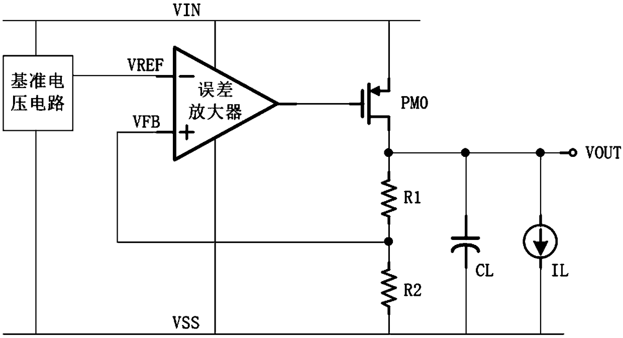
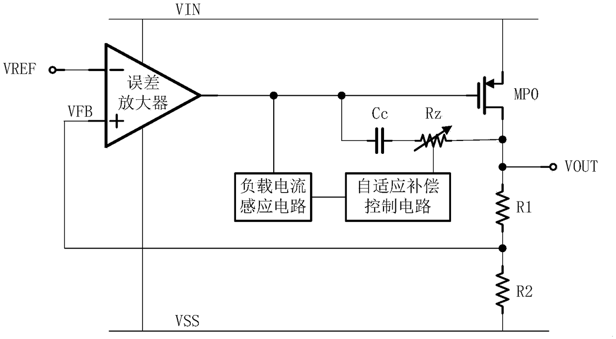
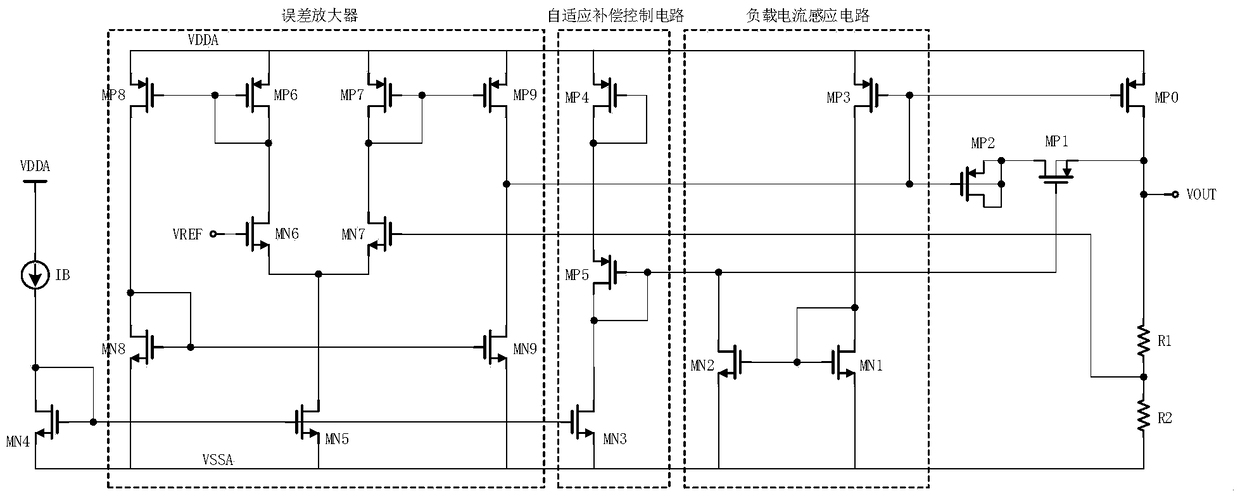
[0028] The present invention proposes a low dropout linear voltage regulator based on adaptive zero point compensation, such as figure 2 As shown, it includes a reference voltage circuit, an error amplifier, a series regulator MPO, and a feedback network composed of a first resistor R1 and a second resistor R2. The inverting input of the error amplifier is connected to the reference voltage circuit, and its non-inverting input is connected to the first One end of the first resistor R1 and one end of the second resistor R2, the output end of which is connected to the gate end of the series adjustment transistor MPO, the source end of the series adjustment transistor MPO is connected to the power supply VIN, and the drain end of the series adjustment transistor MPO is connected to the stable The voltage regulator output terminal VOUT, the other end of the first resistor R1 is connected to the drain end of the series regulator transistor MPO, and the other end of the second resis...
Embodiment 2
[0044] The embodiment of the present invention provides a technical solution: different from embodiment 1, such as Figure 4 Said, the adaptive compensation control circuit includes a fourth PMOS transistor MP4, a fifth PMOS transistor MP5, a third NMOS transistor MN3 and a resistor R0, the drain terminal and the gate terminal of the fourth PMOS transistor MP4 are connected and connected to the The drain end of the third NMOS transistor MN3 is connected, the gate end of the fifth PMOS transistor MP5 is connected to the gate end of the fourth PMOS transistor MP4, and its drain end is respectively connected to one end of the resistor R0 and the second NMOS transistor MP5. The drain end of the transistor MN2 is connected to the gate end of the first PMOS transistor MP1, and the other end of the resistor R0 is grounded, wherein the source terminals of the fourth PMOS transistor MP4 and the fifth PMOS transistor MP5 are connected to a power supply , the source end of the third NMOS...
Embodiment 3
[0048] The embodiment of the present invention provides a technical solution: different from embodiment 1, for the situation of VOUT=VREF in embodiment 1, it can be seen that R1=0, that is, no resistor R1 is needed, only one resistor R2 is needed, but further , considering the actual cost of resistors and process requirements, in the embodiment of the present invention, such as Figure 5 As shown, an NMOS transistor MN0 is used to replace the second resistor R2. Then the low dropout linear regulator further includes a bias circuit and an NMOS transistor MN0 that can be used as an output load, the bias circuit includes a bias current source IB, a fourth NMOS transistor MN4, and the bias current source IB The input terminal is connected to the power supply, the output terminal is connected to the drain terminal of the fourth NMOS transistor MN4, the drain terminal of the fourth NMOS transistor MN4 is connected to the gate terminal, and the source terminal is grounded, the gate t...
PUM
 Abstract
Description
Claims
Application Information