Normally closed field effect transistor

A field effect transistor, normally-off technology, applied in the field of normally-off field effect transistors, can solve the problem of large loss of device performance, and achieve the effects of large saturation current, no loss of device performance, and controllable threshold voltage in an ultra-wide area

Active Publication Date: 2019-01-01
THE 13TH RES INST OF CHINA ELECTRONICS TECH GRP CORP
View PDF4 Cites 2 Cited by
  • Summary
  • Abstract
  • Description
  • Claims
  • Application Information

AI Technical Summary

Problems solved by technology

[0004] The object of the present invention is to provide a kind of normally off type field effect transistor, to solve the technical problem that the sa

Method used


Image

  • Normally closed field effect transistor
  • Normally closed field effect transistor
  • Normally closed field effect transistor

Examples


Embodiment Construction

[0022] In order to make the technical problems, technical solutions and beneficial effects to be solved by the present invention clearer, the present invention will be further described in detail below in conjunction with the accompanying drawings and embodiments. It should be understood that the specific embodiments described here are only used to explain the present invention, not to limit the present invention.

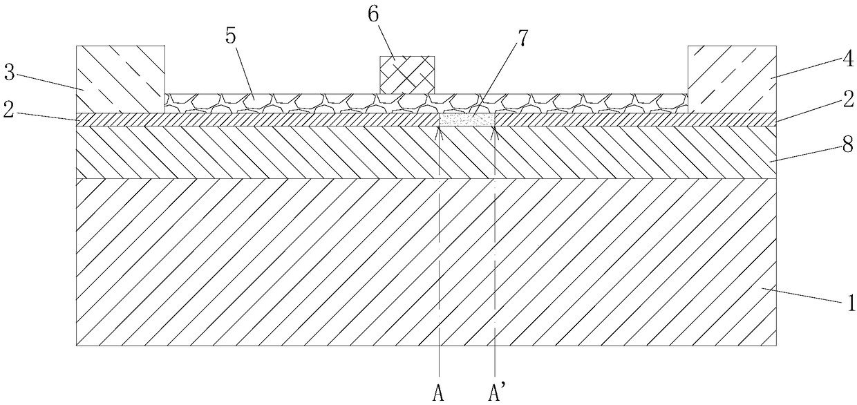
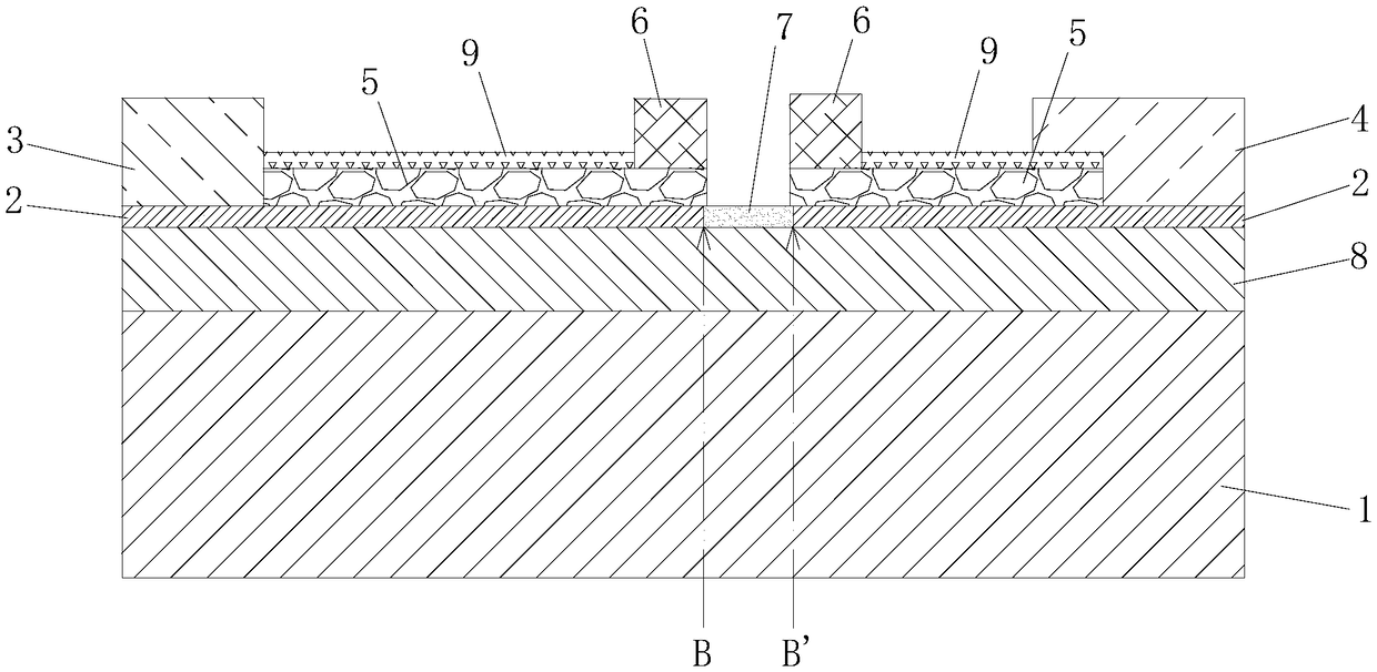
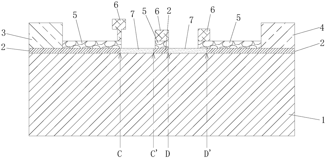
[0023] Please also refer to Figure 1 to Figure 3 , the normally-off field effect transistor provided by the present invention will now be described. The normally-off field effect transistor includes a substrate 1, at least two two-dimensional material layers 2 arranged at intervals on the upper side of the substrate 1, a source electrode 3 arranged on the upper side of the two-dimensional material layer 2, and The drain electrode 4 disposed on the upper side of the two-dimensional material layer 2 and spaced from the source electrode 3, the barrier layer 5 dispos...


PUM

PropertyMeasurementUnit
Widthaaaaaaaaaa
Widthaaaaaaaaaa

Abstract

The present invention provides a normally closed field effect transistor, belonging to the field of semiconductor devices. The normally closed field effect transistor comprises a substrate, at least two two-dimensional material layers mutually arranged at intervals and arranged at the upper side of the substrate, a source electrode arranged at the upper sides of the at least two two-dimensional material layers, a drain electrode arranged at the upper sides of the at least two two-dimensional material layers and arranged at intervals with the source electrode, barrier layers arranged at the upper sides of the at least two two-dimensional material layers and located between the source electrode and the drain electrode and at least one gate electrode arranged at the upper sides of the barrierlayers; and two-dimensional material fault areas are formed between each two adjacent two-dimensional material layers, and the edges of the at least one side of the two-dimensional material fault areas are extruded out of the side edges of projection areas of the gate electrodes on planes where the at least two two-dimensional material layers are located. The normally closed field effect transistor can ensure the migration rate and the electron saturation rate of the device body and has no performance loss while ensuring that the transistor can be pinched off to achieve normal off.

Description

technical field [0001] The invention belongs to the technical field of semiconductor devices, and more specifically relates to a normally-off field effect transistor. Background technique [0002] Two-dimensional nanomaterials refer to materials in which electrons can only move freely (planar motion) on the non-nanoscale (1-100nm) in two dimensions, such as nanofilms. In the past decade, the discovery and research of two-dimensional nanomaterials have made great progress, and two-dimensional nanomaterials including graphene, hexagonal boron nitride, molybdenum disulfide, tungsten disulfide, silicene and germanene have been formed. The development of the entire field of two-dimensional materials has also risen to a new level. Graphene is a typical representative of two-dimensional material devices. It has many excellent physical and chemical properties, and is the thinnest and lightest material currently known, with a thickness of only 0.34nm and a specific surface area of ...

Claims


Application Information

Patent Timeline
IPC IPC(8): H01L29/78H01L29/10
CPCH01L29/1033H01L29/78
Inventor 王元刚冯志红吕元杰房玉龙周幸叶宋旭波谭鑫蔚翠
Owner THE 13TH RES INST OF CHINA ELECTRONICS TECH GRP CORP
Why Eureka
Try Eureka