Supercharge Your Innovation With Domain-Expert AI Agents!

MOS transistor driver circuit

A drive circuit and MOS tube technology, applied in electrical components, output power conversion devices, etc., can solve the problems of slow switching speed of IGBT drive circuit, poor electrical isolation performance of MOS tube rapid shutdown, and prone to false triggering, etc., to achieve Enhanced anti-interference characteristics, easy development and use, and fast switching speed

Inactive Publication Date: 2019-01-04
SHANGHAI LYNAC NUMERICAL CONTROL TECH CO LTD
View PDF8 Cites 2 Cited by
  • Summary
  • Abstract
  • Description
  • Claims
  • Application Information

AI Technical Summary

Problems solved by technology

[0005] The technical problem to be solved by the present invention is to overcome the slow switching speed of the IGBT drive circuit in the prior art, the driving duty cycle of the MOSFET bootstrap circuit cannot reach 100%, and the complementary output circuit composed of triodes cannot provide negative voltage shutdown to ensure that the MOS tube With the defects of rapid shutdown, poor electrical isolation performance, and prone to false triggering, a MOS tube drive circuit is provided

Method used


Image

  • MOS transistor driver circuit
  • MOS transistor driver circuit

Examples


Embodiment 1

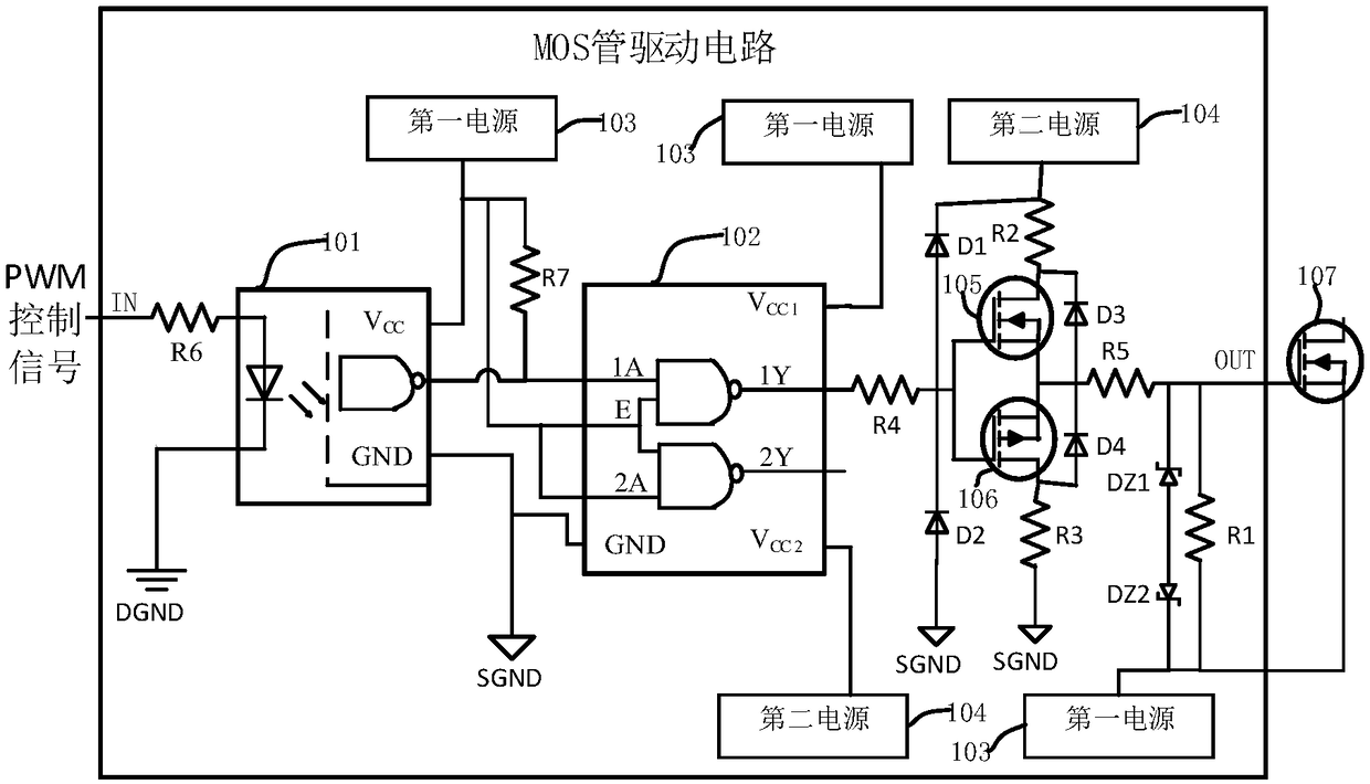
[0021] The MOS transistor drive circuit of this embodiment, such as figure 1 As shown, the driving circuit is used to drive the target NMOS transistor 107. The driving circuit includes a photocoupler 101, a level driver 102, an NMOS transistor 105, a PMOS transistor 106, and a first resistor R1. The photocoupler 101 The anode is connected to the PWM control signal input end, the cathode is grounded, the collector of the optocoupler 101 is respectively connected to the input end of the level driver 102 and the first power supply 103, and the emitter of the optocoupler 101 is grounded. The output terminals of the level driver 102 are respectively connected to the gate of the NMOS transistor 105 and the gate of the PMOS transistor 106, the drain of the NMOS transistor 105 is connected to the second power supply 104, and the PMOS transistor 106 The drain of the NMOS transistor 105, the source of the PMOS transistor 106, and one end of the first resistor R1 are all connected to the...

Embodiment 2

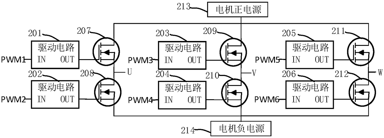
[0039] In this embodiment, six MOS transistor driving circuits as in Embodiment 1 are used to drive six target NMOS transistors, thereby forming a driving circuit capable of driving a three-phase motor. Such as figure 2 As shown, the drive circuits 201-206 are the MOS transistor drive circuits of Embodiment 1, and the external PWM1-PWM6 control signals pass through the input terminals of the drive circuits 201-206 respectively (such as figure 2 IN shown) is input into the driving circuits 201-206, and then through the output terminals of the driving circuits 201-206 (such as figure 2 OUT shown) to respectively drive the target NMOS tubes 207-212, the motor positive power supply 213 and the motor negative power supply 214 provide power for the target NMOS tubes 207-212, and U, V, W are respectively connected to the U of the three-phase motor. phase, V phase, W phase. figure 2 In the above, for the sake of simplicity and clarity, the connection between the sources of the t...


PUM


Abstract

A MOS transistor drive circuit is disclosed, and is used for driving a target NMOS transistor. A circuit comprises a photoelectric coupler, a level driver, an NMOS transistor, a PMOS transistor, and first resistor, the anode of the photoelectric coupler is connected with a control signal input terminal, the cathode is connected to the ground, the collector of the photoelectric coupler is respectively connected with an input terminal of the level driver and a first power supply, the emitter of the photoelectric coupler is connected to the ground, the output terminal of the level driver is connected with the grid of the NMOS transistor and the grid of the PMOS transistor separately, the drain of the NMOS transistor is connected to a second power supply, the drain of the PMOS transistor is grounded, the source of the NMOS transistor, the source of the PMOS transistor and one end of the first resistor are connected to the grid of the target NMOS transistor, and the other end of the first resistor and the source of the target NMOS transistor are connected to the first power supply. The invention has the advantages of high switching speed, the duty cycle can reach 100%, a negative voltage shutdown function is achieved, electrical isolation is good and the circuit is not liable to be interfered.

Description

technical field [0001] The invention belongs to the field of motor drive, in particular to a MOS tube drive circuit. Background technique [0002] With the rapid development of power electronic devices, the power drive technology has risen rapidly. As one of the main components of the servo drive device, the performance of the motor driver directly affects the performance of the CNC machine tool. The power drive circuit is the most important power conversion link in the motor driver, which plays an absolute role in the performance of the motor driver. [0003] Traditional power driving circuits are mostly based on IGBT (Insulated Gate Bipolar Transistor, insulated gate bipolar transistor) driving circuits. However, due to its own structural problems, the switching speed of IGBT is slow, generally only 10kHz ~ 20kHz, it is difficult to meet some power device driving occasions with specific switching speed requirements, and the driving circuit based on MOSFET (Metal-Oxide Se...

Claims


Application Information

Patent Timeline
IPC IPC(8): H02M1/088
CPCH02M1/088
Inventor 周兴鹏袁再松
Owner SHANGHAI LYNAC NUMERICAL CONTROL TECH CO LTD
Features
  • R&D
  • Intellectual Property
  • Life Sciences
  • Materials
  • Tech Scout
  • Unparalleled Data Quality
  • Higher Quality Content
  • 60% Fewer Hallucinations
Learn More