

Bonding-based thin film bulk acoustic wave resonator based and processing method thereof
A thin-film bulk acoustic wave and processing method technology, which is applied in the field of piezoelectric devices, can solve the problems affecting the performance of thin-film bulk acoustic wave resonators and difficult removal of sacrificial layer materials, so as to avoid incomplete release and improve the Q value
- Summary
- Abstract
- Description
- Claims
- Application Information
AI Technical Summary
Problems solved by technology
Method used
Image

Examples
Embodiment 1
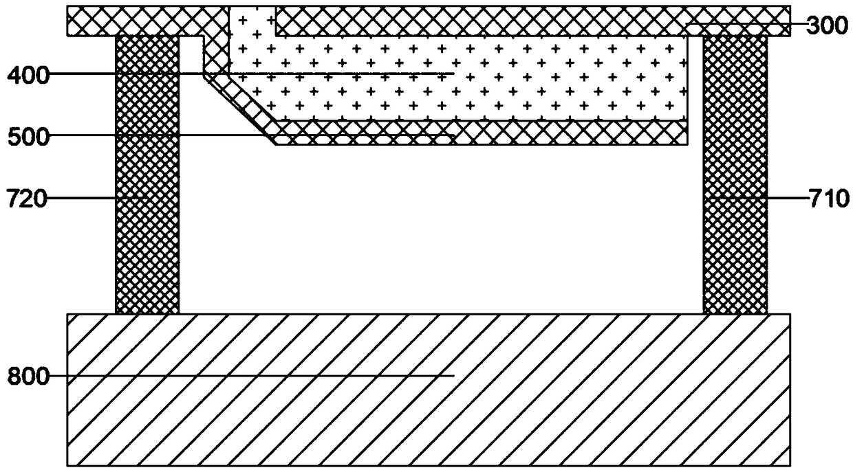
[0043] The present invention proposes a novel bonding-based film bulk acoustic resonator, the specific structure of which can be found in figure 1 shown. It includes: a substrate 100 , a first metal pillar 710 and a second metal pillar 720 arranged on the substrate 100 , and a pressure rod arranged between the first metal pillar 710 and the second metal pillar 720 An electrical film stack structure, wherein the piezoelectric film stack structure includes a first electrode 300, a piezoelectric layer 400, and a second electrode 500, and the piezoelectric layer 400 is located at the first electrode 300 and the second electrode 500 Between, and the first electrode 300 and the second electrode 500 are arranged opposite, the first electrode 300 is also electrically connected to the first metal post 710, and the second electrode 500 is also connected to the second The metal posts 720 are electrically connected.
[0044] The bonding-based thin-film bulk acoustic resonator of the emb...
Embodiment 2
[0050] Referring to FIG. 2, the bonding-based thin-film bulk acoustic resonator according to Embodiment 1 of the present invention can be manufactured through the following process steps:
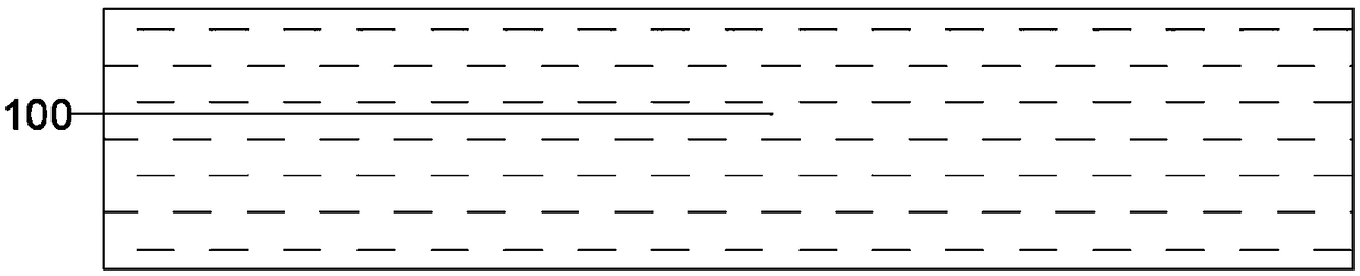
[0051] A silicon wafer polished on one side or both sides is prepared as the substrate 100 with the polished side facing up, and standard cleaning is performed, as shown in FIG. 2( a ).
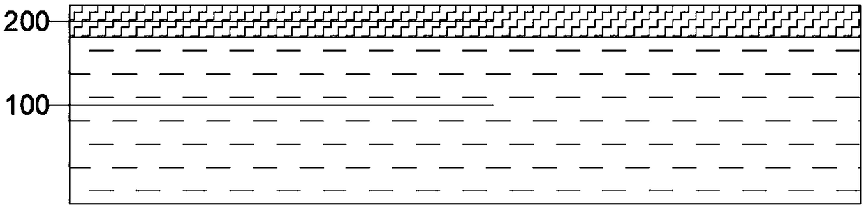
[0052] Electrode materials and piezoelectric materials are deposited on the substrate 100 to construct a piezoelectric film stack structure, wherein the piezoelectric film stack structure includes a first electrode 300, a piezoelectric layer 400 and a second electrode 500, and the piezoelectric layer 400 is located between the first electrode 300 and the second electrode 500, and the first electrode 300 and the second electrode 500 are oppositely arranged.
[0053] Preferably, in order to facilitate the peeling of the substrate 100 after eutectic bonding, in the manufacturing process of the bonded thin-film ...
PUM
 Abstract
Description
Claims
Application Information