Array substrate, manufacturing method thereof, and display panel

A technology of an array substrate and a manufacturing method, applied in the display field, can solve the problems of unstable channel layer performance, numerous manufacturing processes, and inability to reduce production costs, and achieve the effects of stable performance and reduction of mask manufacturing processes.

Active Publication Date: 2020-11-10
TCL CHINA STAR OPTOELECTRONICS TECH CO LTD
View PDF6 Cites 0 Cited by
  • Summary
  • Abstract
  • Description
  • Claims
  • Application Information

AI Technical Summary

Problems solved by technology

However, the preparation of an array substrate (Array substrate) with a gate-type TFT on the top requires more mask (Mask) processes, resulting in a large number of manufacturing processes, which cannot reduce production costs, and the channel layer is easily affected by light and has unstable performance.

Method used


Image

  • Array substrate, manufacturing method thereof, and display panel
  • Array substrate, manufacturing method thereof, and display panel
  • Array substrate, manufacturing method thereof, and display panel

Examples


Embodiment Construction

[0028] The following clearly and completely describes the technical solutions of each exemplary embodiment provided in the present application with reference to the drawings in the embodiments of the present application. In the case of no conflict, the following embodiments and features in the embodiments can be combined with each other. Moreover, the directional terms used throughout the application, such as "up", "down", etc., are for better describing the technical solutions of various embodiments, and are not used to limit the protection scope of the application.

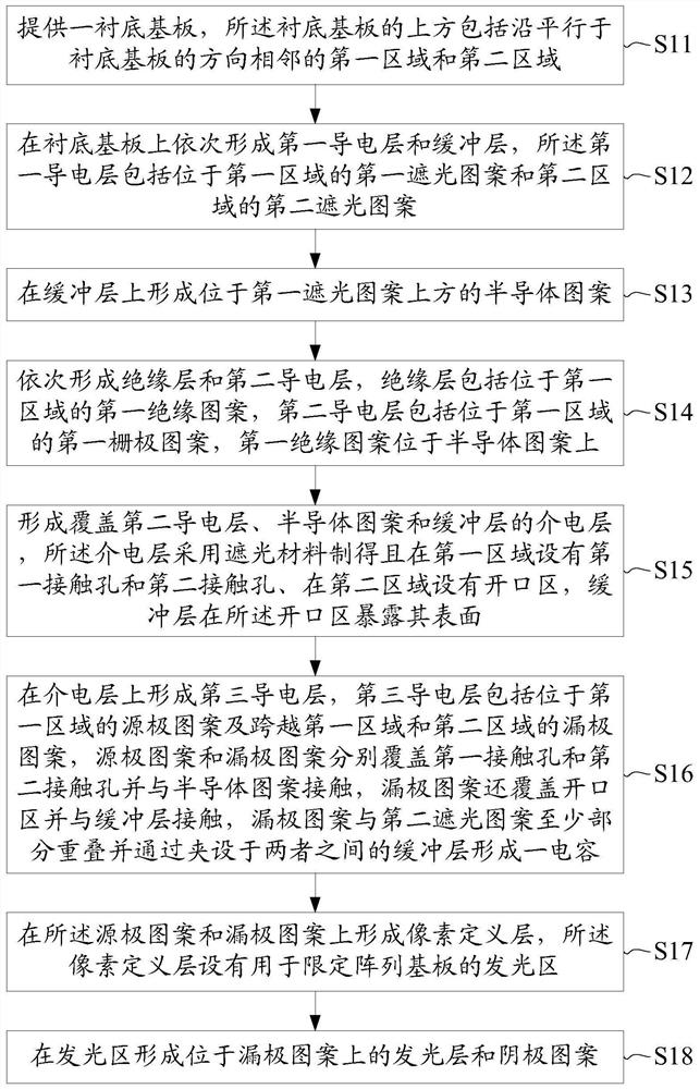
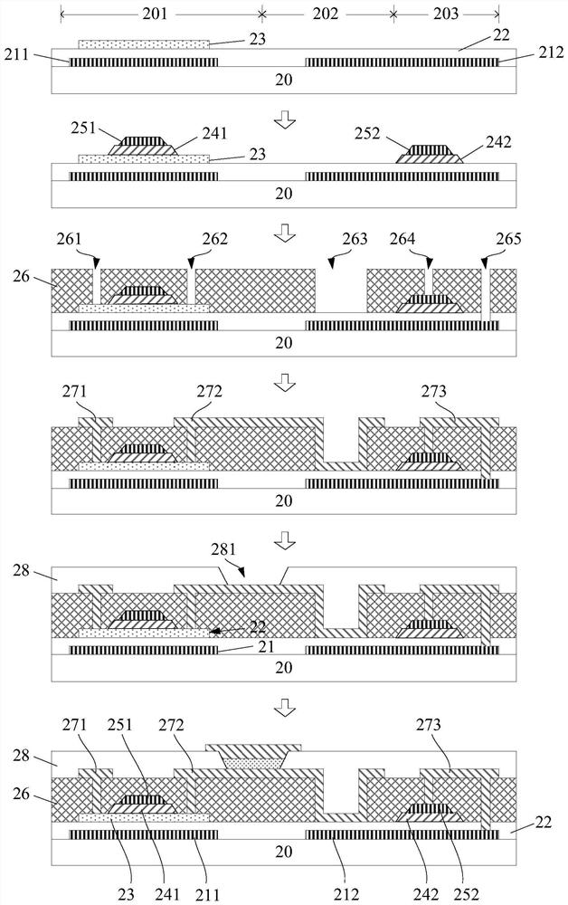
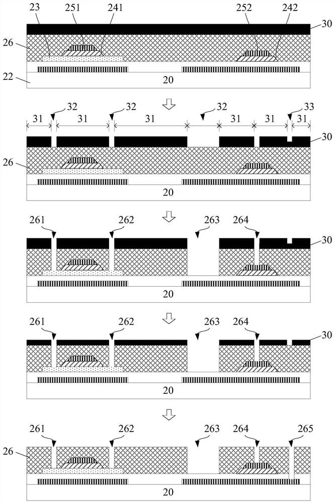
[0029] figure 1 is a schematic flow chart of an embodiment of the manufacturing method of the array substrate of the present application, figure 2 is based on figure 1 Schematic diagram of the fabrication of the array substrate by the method shown. combine figure 1 and figure 2 As shown, the manufacturing method may include the following steps S11-S18.

[0030] S11: Provide a base substrate, above which ...


PUM

PropertyMeasurementUnit
thicknessaaaaaaaaaa

Abstract

The application discloses an array substrate, a manufacturing method thereof, and a display panel. In this application, the source pattern and the drain pattern are designed to be directly formed on the dielectric layer, and the traditional flat layer and passivation layer are replaced by the dielectric layer, and the drain pattern is also used as the anode pattern of the OLED device, thereby reducing the The photomask process, and the dielectric layer is made of a light-shielding material, which can protect the channel layer of the TFT from being affected by light, and is beneficial to ensure its stable performance.

Description

technical field [0001] The present application relates to the display field, in particular to an array substrate, a manufacturing method thereof, and a display panel. Background technique [0002] Currently, the TFT (Thin Film Transistor, thin film transistor) whose channel layer is made of metal oxide (Oxide) semiconductor has been widely used in OLED (Organic Light-Emitting Diode, Organic Light-Emitting Diode) display panels, in which the top gate Type TFT has become the industry's first choice due to its small parasitic capacitance. However, the preparation of the array substrate (Array substrate) with gate-type TFTs on top requires many mask (Mask) processes, resulting in complicated manufacturing processes, which cannot reduce production costs, and the channel layer is easily affected by light and has unstable performance. Contents of the invention [0003] In view of this, the present application provides an array substrate, a manufacturing method thereof, and a dis...

Claims


Application Information

Patent Timeline
Patent Type & Authority Patents(China)
IPC IPC(8): H01L27/12H01L27/32H01L29/417H01L29/786H01L51/52H01L51/56H01L21/84H01L21/44H01L21/34
CPCH01L27/1248H01L27/1259H01L29/401H01L29/41733H01L29/66969H01L29/78633H10K59/1213H10K50/81H10K59/1201H10K71/00
Inventor 周星宇
Owner TCL CHINA STAR OPTOELECTRONICS TECH CO LTD
Why Eureka
Try Eureka