A thick film substrate miniaturized metal tube shell encapsulation structure

A packaging structure and metal tube technology, applied in the structural connection of printed circuits, printed circuits connected with non-printed electrical components, electrical components, etc., can solve the problems of inability to bond components and low circuit integration, and achieve The effect of reducing the difficulty of testing and simple assembly

Pending Publication Date: 2019-01-18
NORTH ELECTRON RES INST ANHUI CO LTD
View PDF0 Cites 7 Cited by
  • Summary
  • Abstract
  • Description
  • Claims
  • Application Information

AI Technical Summary

Problems solved by technology

[0003] Disadvantages: A single substrate is bonded to a metal tube package, so that the back of the substrate cannot be bonded with components, and only the front of the substrate can be assembled with surface mount devices or bare chips, resulting in a low degree of circuit integration

Method used


Image

  • A thick film substrate miniaturized metal tube shell encapsulation structure
  • A thick film substrate miniaturized metal tube shell encapsulation structure
  • A thick film substrate miniaturized metal tube shell encapsulation structure

Examples


Embodiment Construction

[0028] The present invention will be further described below in conjunction with the accompanying drawings. The following examples are only used to illustrate the technical solution of the present invention more clearly, but not to limit the protection scope of the present invention.

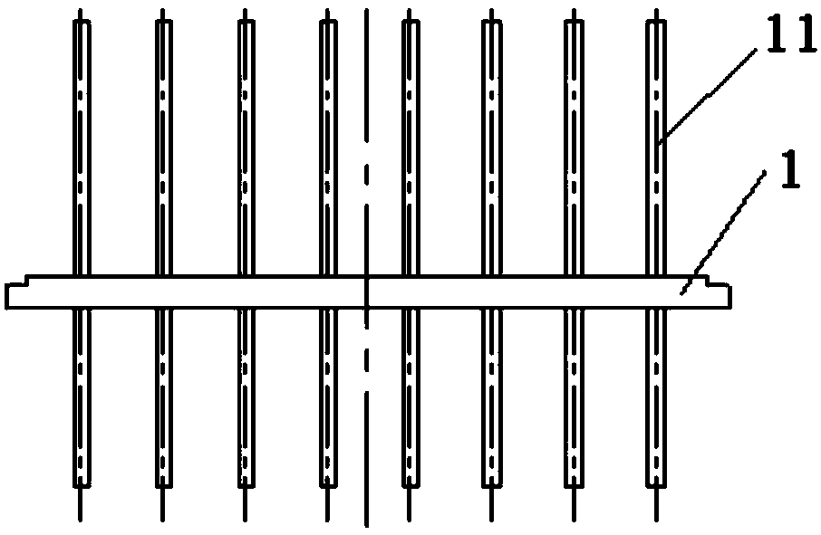
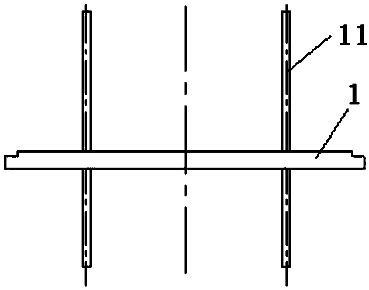
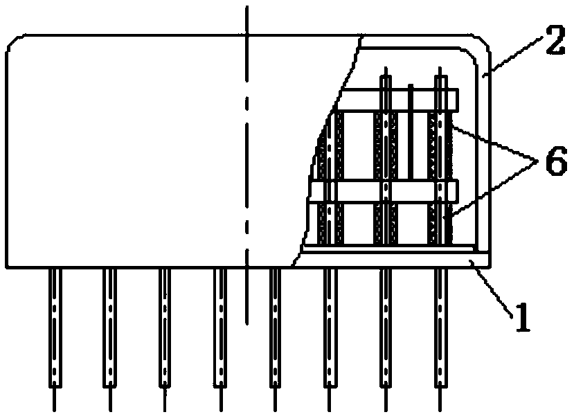
[0029] combine figure 1 - Figure 4 In the present invention, the ceramic substrate and the printed board are mixed and assembled in the shell base, and the shell base 1 and the metal cap 2 are welded by laser to form a fully airtight package. Thick film and printed board miniaturized metal shell packaging design technology uses 2-layer PCB boards to be packaged on the pins of the shell base by soldering. The front and back of the lower PCB board 3 are completely surface-mounted, and the upper PCB board 4 Surface-mount parts are also used on the front and back, wherein a ceramic substrate 5 is welded to the front (upper surface) of the upper PCB board. The ceramic substrate 5 adopts a thick f...


PUM


Abstract

The invention discloses a thick film substrate miniaturized metal tube encapsulation structure. Upper layer and lower layer PCB boardS with a set distance are sleeved on the pins of the tube case base, and the upper layer and the lower layer PCB boards are electrically connected through pins or pins. The upper and / or lower surfaces of the lower two layers of PCB are provided with surface mountingelements. A ceramic substrate is soldered to the upper surface of the upper PCB, and a metal cap is covered on the base of the shell to seal the two layers of PCB. The circuit unit and the resistor which require high resistance precision are printed on the ceramic substrate by adopting a thick film process, which is favorable for active fine adjustment of the resistor and easy operation; Reasonable division of circuit layout is conducive to the circuit performance test of each board and reduces the difficulty of test.

Description

technical field [0001] The invention relates to a miniaturized metal shell packaging structure of a thick film substrate. Background technique [0002] At present, the known thick film substrate assembly metal shell structure packaging technology is generally to assemble the surface mount device or bare chip on the front of the substrate; then the back of the substrate is fixed to the shell by bonding, and finally the shell and the metal cover Parallel seam welding is carried out to realize the fully airtight packaging structure of the metal shell. [0003] Disadvantages: A single substrate is bonded to a metal tube package, so that the back of the substrate cannot be bonded with components, and only the front of the substrate can be assembled with surface-mounted devices or bare chips, resulting in a low degree of circuit integration. Contents of the invention [0004] The purpose of the present invention is to provide a thick-film substrate miniaturized metal shell pack...

Claims


Application Information

Patent Timeline
Patent Type & Authority Applications(China)
IPC IPC(8): H01L23/31H01L23/522H05K1/14H05K1/18
CPCH01L23/3121H01L23/522H05K1/144H05K1/18
Inventor 聂月萍
Owner NORTH ELECTRON RES INST ANHUI CO LTD
Why Eureka
Try Eureka